

- RFQ
- BOM
-
Contact Us
Tel: +86-0755-83501315
Email: sales@sic-components.com


- Chinese
- English
- French
- German
- Portuguese
- Spanish
- Russian
- Japanese
- Korean
- Arabic
- Irish
- Greek
- Turkish
- Italian
- Danish
- Romanian
- Indonesian
- Czech
- Afrikaans
- Swedish
- Polish
- Basque
- Catalan
- Esperanto
- Hindi
- Lao
- Albanian
- Amharic
- Armenian
- Azerbaijani
- Belarusian
- Bengali
- Bosnian
- Bulgarian
- Cebuano
- Chichewa
- Corsican
- Croatian
- Dutch
- Estonian
- Filipino
- Finnish
- Frisian
- Galician
- Georgian
- Gujarati
- Haitian
- Hausa
- Hawaiian
- Hebrew
- Hmong
- Hungarian
- Icelandic
- Igbo
- Javanese
- Kannada
- Kazakh
- Khmer
- Kurdish
- Kyrgyz
- Latin
- Latvian
- Lithuanian
- Luxembou..
- Macedonian
- Malagasy
- Malay
- Malayalam
- Maltese
- Maori
- Marathi
- Mongolian
- Burmese
- Nepali
- Norwegian
- Pashto
- Persian
- Punjabi
- Serbian
- Sesotho
- Sinhala
- Slovak
- Slovenian
- Somali
- Samoan
- Scots Gaelic
- Shona
- Sindhi
- Sundanese
- Swahili
- Tajik
- Tamil
- Telugu
- Thai
- Ukrainian
- Urdu
- Uzbek
- Vietnamese
- Welsh
- Xhosa
- Yiddish
- Yoruba
- Zulu
- Kinyarwanda
- Tatar
- Oriya
- Turkmen
- Uyghur
- Tag List
- N-Channel MOSFET: A Comprehensive Analysis of Structure, Working Principles, Types, and Applications
N-Channel MOSFET: A Comprehensive Analysis of Structure, Working Principles, Types, and Applications
1. Fundamental Understanding of N-Channel MOSFETs
1.1 Overview of MOSFETs https://www.sic-components.com/single-fets-mosfets
A MOSFET (Metal-Oxide-Semiconductor Field-Effect Transistor) is a critical semiconductor device that amplifies or switches electrical signals. It consists of a metal gate, an insulating oxide layer (typically silicon dioxide), and a semiconductor substrate (usually silicon). This structure enables precise control over current flow. For example, a planar N-channel enhancement-mode NMOSFET features a P-type silicon substrate with two diffused N-type regions (source and drain) on its surface. A silicon dioxide (SiO₂) insulating layer covers these regions, with metal electrodes for the gate (G), source (S), and drain (D) formed via etching and metallization. The gate is electrically isolated from the drain and source, while the drain-source path contains two PN junctions—however, the substrate is internally connected to the source, effectively leaving one PN junction between drain and source. This structure forms the basis for its unique electrical properties.
1.2 Definition of N-Channel MOSFETs
An N-channel MOSFET is a type of MOSFET where electrons serve as the primary charge carriers. When activated, current flow is driven by electron movement through the channel, contrasting with P-channel MOSFETs (which use holes as carriers). In an N-channel MOSFET, a silicon dioxide layer on the substrate provides electrical insulation, with metal layers on top forming the gate, source, and drain regions—hence the abbreviation "NMOS". The use of electrons as carriers gives N-channel MOSFETs superior mobility and performance in various applications.
2. Types of N-Channel MOSFETs
2.1 Enhancement-Mode N-Channel MOSFETs
Structure
Enhancement-mode N-channel MOSFETs use a P-type silicon substrate with two heavily doped N-type regions embedded as the source and drain electrodes. The area between source and drain is the channel region, defined by length (l) and width (w). A thin silicon dioxide (SiO₂) insulating layer covers the substrate and extends over the source-drain region, with a metal layer above forming the gate, source, and drain electrodes.
Working Principle
Off State (VGS = 0): No conductive channel exists between source and drain, so no current (ID) flows, and the MOSFET is off.
Channel Formation (VGS > VTH): Applying a positive voltage (VGS) between the gate and source generates an electric field that attracts electrons from the N-type source region toward the oxide layer. When VGS exceeds the threshold voltage (VTH), enough electrons accumulate under the oxide layer to form an N-type conductive channel, connecting source and drain.
On State (VGS > VTH + VDS): With a channel established, applying a voltage (VDS) between drain and source allows electrons to flow from source to drain, creating ID. The channel conductivity is proportional to VGS—higher VGS increases conductivity and ID. Reducing or removing VGS collapses the channel, turning the MOSFET off.
Characteristics
Transfer Characteristics: Plots ID vs. VGS. ID is near-zero when VGS < VTH; ID increases rapidly as VGS ≥ VTH, with the curve lying in the positive voltage region.
Output Characteristics: Plots ID vs. VDS for different VGS values. At low VDS, ID linearly relates to VDS (linear region, acting as a variable resistor). As VDS reaches VGS - VTH, the channel pinches off, and ID saturates (saturation region, acting as a current source controlled by VGS).
2.2 Depletion-Mode N-Channel MOSFETs
Structure
Depletion-mode N-channel MOSFETs also use a P-type silicon substrate with heavily doped N-type source and drain regions. Unlike enhancement-mode devices, their manufacturing process introduces metal positive ions into the SiO₂ layer under the gate, inducing negative ions beneath the oxide and pre-forming a conductive channel between source and drain (length l, width w).
Working Principle
On State (VGS = 0): A pre-existing channel allows current (ID) to flow when VDS is applied, even with zero gate voltage.
Channel Modulation (VGS ≠ 0): Applying a negative VGS repels channel electrons, reducing electron density, increasing channel resistance, and decreasing ID. At the pinch-off voltage (VP), the channel disappears, turning the MOSFET off. Applying positive VGS increases electron density, enhancing channel conductivity and ID.
Characteristics
Transfer Characteristics: Plots ID vs. VGS, showing an initial current (IDSS) at VGS = 0. ID decreases as VGS becomes negative (toward VP) and increases as VGS becomes positive.
Output Characteristics: For different VGS values, ID linearly relates to low VDS and saturates at higher VDS. Depletion-mode devices conduct at VGS = 0 and offer flexible current control via VGS polarity and magnitude.
3. In-Depth Working Principles of N-Channel MOSFETs
3.1 Working Process of Enhancement-Mode MOSFETs
Off State (VGS = 0)
With VGS = 0, the P-type substrate between the N-type source and drain regions blocks conduction. The reverse-biased PN junction between drain and substrate prevents current flow, keeping ID ≈ 0.
Channel Formation (VGS Increases to > VTH)
Treating the gate and substrate as a capacitor with the oxide layer as dielectric, increasing VGS induces positive charges on the gate-oxide interface and negative charges (inversion layer) on the oxide-substrate interface. At low VGS, few negative charges form, neutralized by holes in the P-type substrate. At VGS = VTH, enough negative charges accumulate to connect the N-type source and drain, forming an N-channel. Further increasing VGS expands the channel and reduces resistance.
On State (VGS > VTH + Applied VDS)
With a conductive channel, applying VDS drives electrons from source to drain via the channel, creating ID. ID depends on both VDS and VGS—higher VGS enhances channel conductivity, increasing ID.
3.2 Key Factors Influencing Working Characteristics
Gate-Source Voltage (VGS): Controls device state. For enhancement-mode, VGS > VTH is required to turn on, with VGS directly affecting channel conductivity and ID. For depletion-mode, VGS adjusts channel carrier density to control ID.
Drain-Source Voltage (VDS): Determines carrier driving force. In the linear region, ID ∝ VDS; in the saturation region, ID stabilizes with increasing VDS.
Threshold Voltage (VTH): A critical parameter for enhancement-mode devices, defining the VGS threshold for channel formation. VTH varies by device and is vital for design and selection.
Channel Resistance (RDS): Affects conduction loss. Lower RDS reduces voltage drop and power dissipation, improving efficiency. RDS depends on channel dimensions, doping concentration, and VGS.
4. Application Fields of N-Channel MOSFETs
4.1 Power Management
DC-DC Converters: As switching elements in DC-DC converters (e.g., Buck converters), N-channel MOSFETs regulate input DC voltage to a stable output. During conduction, they charge an inductor; during cutoff, the inductor sustains load current. Their high switching speed enables efficient power conversion with minimal loss.
Battery Protection Circuits: N-channel MOSFETs protect batteries from overcharge, overdischarge, and overcurrent. When detected, the control circuit turns off the MOSFET to disconnect the battery, extending its lifespan.
4.2 Motor Drive
DC Motor Drive: In H-bridge circuits for DC motor control, N-channel MOSFETs enable forward/reverse rotation and speed regulation by switching conduction states. In electric vehicle drives, they precisely control motor torque and speed for smooth operation.
Stepper Motor Drive: N-channel MOSFETs control stepper motor phases to achieve precise angle and speed control, essential for 3D printers, CNC machines, and other precision equipment.
4.3 Signal Processing and Amplification
Audio Amplifiers: As core elements in audio amplifiers, N-channel MOSFETs leverage their saturation-region current source characteristics to linearly amplify weak audio signals, offering low distortion and high efficiency for superior sound quality.
RF Amplifiers: In RF communication systems, N-channel MOSFETs excel in RF amplification due to high electron mobility and switching speed, enabling stable high-frequency signal amplification in devices like mobile phones and base stations.
4.4 Other Applications
Lighting Control: Combined with PWM technology, N-channel MOSFETs adjust LED brightness by controlling conduction time, enabling energy-efficient and precise dimming in smart lighting systems.
Computer Motherboards: N-channel MOSFETs manage power switching and signal transmission in motherboard circuits (e.g., CPU power supply control, memory/USB interface signal switching), ensuring stable system operation.
5. Advantages of N-Channel MOSFETs
5.1 Performance Benefits of High Electron Mobility
N-channel MOSFETs feature higher electron mobility than P-channel devices (2-3 times higher for the same RDS(on)), enabling lower conduction loss and higher efficiency. In high-power applications, this reduces heat dissipation requirements, cutting system cost and size.
5.2 Superior Switching Characteristics
Fast Switching Speed: N-channel MOSFETs switch states in nanoseconds, ideal for high-frequency applications (e.g., switching power supplies, PWM circuits). Faster switching allows higher operating frequencies, reducing inductor/capacitor sizes for compact, efficient designs.
Low Switching Loss: Rapid switching minimizes overlap between current and voltage during transitions, reducing switching loss. This is crucial for high-frequency, high-current applications, improving system stability by lowering device temperature.
5.3 Low Gate Drive Current
The insulated gate structure of N-channel MOSFETs results in extremely high input impedance, requiring minimal gate current. This allows direct driving by low-power devices (e.g., microcontrollers), simplifying circuit design and reducing system power consumption.
5.4 Compatibility with IC Processes
N-channel MOSFET manufacturing processes are highly compatible with modern IC technologies, enabling integration of multiple MOSFETs and other devices on a single chip. This compatibility is fundamental for constructing logic gates and circuit modules in large-scale ICs (e.g., microprocessors, memories), driving miniaturization and high-performance development in electronic products.
6. Selection Guidelines for N-Channel MOSFETs
6.1 Consideration of Rated Voltage Parameters
Drain-Source Breakdown Voltage (V(BR)DSS): The maximum voltage the drain-source can withstand without breakdown. Select a MOSFET with V(BR)DSS > the maximum circuit VDS, accounting for voltage spikes (e.g., from inductive loads in switching power supplies). A safety margin of 20-30% is recommended (e.g., choose V(BR)DSS ≥ 60V for a 48V system).
Gate-Source Voltage (VGS) Rating: The maximum VGS to prevent oxide layer breakdown. Ensure the drive voltage does not exceed this rating (e.g., 20V for standard MOSFETs, 12V for logic-level devices).
6.2 Current Parameters
Continuous Drain Current (ID): The maximum continuous current the MOSFET can handle without damage. Select an ID rating 20-50% higher than the circuit’s maximum current (e.g., ID ≥ 6A for a 4A load) to avoid overheating.
Pulse Drain Current (IDM): The maximum transient current for short periods (e.g., during motor starting). Ensure IDM ≥ peak transient current.
6.3 On-Resistance (RDS(on))
RDS(on) directly impacts conduction loss (P = ID² × RDS(on)). For high-efficiency applications, choose MOSFETs with low RDS(on) (e.g., < 10mΩ for high-current switches). Note that RDS(on) increases with temperature, so derate for high-temperature environments.
6.4 Threshold Voltage (VTH)
Logic-Level vs. Standard MOSFETs: Logic-level MOSFETs turn on fully at 3.3V/5V (VTH ≤ 2V), suitable for microcontroller-driven circuits. Standard MOSFETs require VGS ≥ 10V for full conduction.
Consistency: Ensure VTH tolerance matches circuit requirements (e.g., ±0.5V for precise control).
6.5 Gate Charge (QG)
QG affects switching speed (higher QG = slower switching). For high-frequency applications (e.g., > 100kHz), choose MOSFETs with low QG (e.g., QG ≤ 10nC) to minimize switching loss.
6.6 Thermal Management
Thermal Resistance (RθJA): Determines heat dissipation capability. Lower RθJA (e.g., < 50°C/W) reduces temperature rise. For high-power applications, use heat sinks and ensure proper airflow.
Junction Temperature (Tj): Must remain below the maximum rating (typically 150°C). Calculate Tj = TA + (P × RθJA) and ensure Tj < Tj(max).
6.7 Packaging and Application Requirements
Package Type: SMD packages (e.g., TO-220, DPAK) for compact designs; through-hole packages for high-power applications.
Environmental Ratings: Consider humidity, temperature, and vibration resistance for industrial or automotive use.
7. Conclusion
N-channel MOSFETs are indispensable in modern electronics, driving innovation across power management, motor control, and signal processing. Their high electron mobility, fast switching, and low drive current make them ideal for efficient, compact designs. When selecting an N-channel MOSFET, prioritize voltage/current ratings, RDS(on), VTH, and thermal characteristics to ensure optimal performance. As technology advances—toward wider bandgap materials (e.g., GaN, SiC) and integrated power modules—N-channel MOSFETs will continue to play a pivotal role in shaping the future of electronics, enabling higher efficiency and smarter designs.
https://www.sic-components.com/single-fets-mosfets
Hot Products
View More-

SRT6442WC1D02GE064P00IE SolidRun LTD
-
EDM1CFIMX6U10R1GBNI4GL2C TechNexion
-
SRMX6QDWT1D02GE064E01IE SolidRun LTD
-
SRMM8QDW00D01GE064R02IH SolidRun LTD
-
SRMX6DUW00D01GE016V20A0 SolidRun LTD
-
SRMP8DUWB1D02GE128V12C0 SolidRun LTD
-
SRMX6DLW00D01GE064G01CH SolidRun LTD
-
SRS9130S00D04GE008P01IH SolidRun LTD
-
SRMP8QDWB1D04GE016U03CH SolidRun LTD
-
SRMX6SOW00D256E008G01IE SolidRun LTD
-
SRMP8QLW00D03GE064V12I0 SolidRun LTD
-
SRS9130S00D02GE008P01IH SolidRun LTD
Related Blogs
-
2025 / 07 / 09
CD4007: A Comprehensive Analysis of a Multifunctional CMOS Integrated Circuit
In the field of modern electronic technology, CMOS (Complementary Metal-Oxide-Semiconductor) integrated circuits have become core components in digital and analog circuit design due to their low power consumption, high integration, and excellent compatibility. As a classic CMOS device, the CD4007 oc...
-
2025 / 07 / 07
Understanding IC 7408: A Fundamental Component in Digital Logic Design
In the vast and intricate realm of digital electronics, integrated circuits (ICs) serve as the building blocks that enable the creation of complex and powerful systems. Among these, the IC 7408 holds a special place as a fundamental component in digital logic design. This article aims to provide a c...
-
2025 / 07 / 04
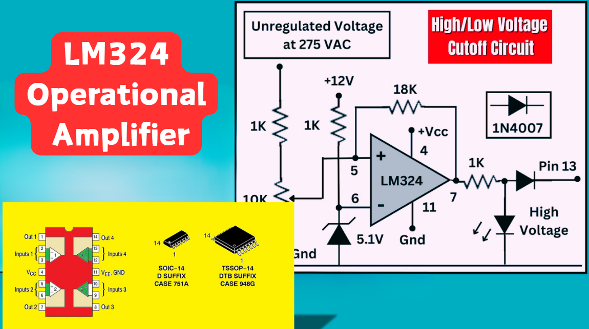
LM324 Operational Amplifier Comprehensive Guide: Pins, Applications, Packaging, and Datasheet
The LM324 is a low-cost integrated circuit featuring four independent operational amplifiers (op-amps), renowned for its wide voltage adaptability, low power consumption, and high reliability in industrial and consumer electronics. With a single-supply voltage range of 3V to 32V (or dual-supply rang...
-
2025 / 07 / 02
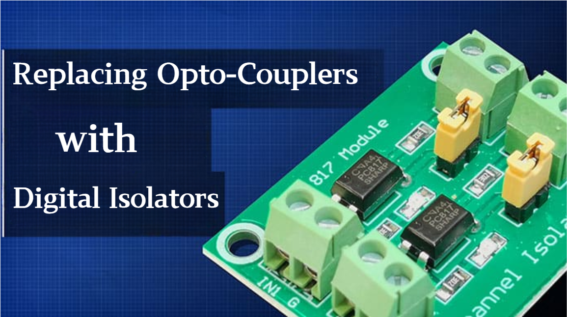
A Comprehensive Guide to Replacing Opto-Couplers with Digital Isolators: From Principles to Practice
In the ever-evolving landscape of electronic design, the transition from opto-couplers to digital isolators marks a pivotal shift in isolation technology. For decades, opto-couplers have been the cornerstone of electrical isolation in industrial control, medical devices, and power systems, relying o...
-
2025 / 06 / 30
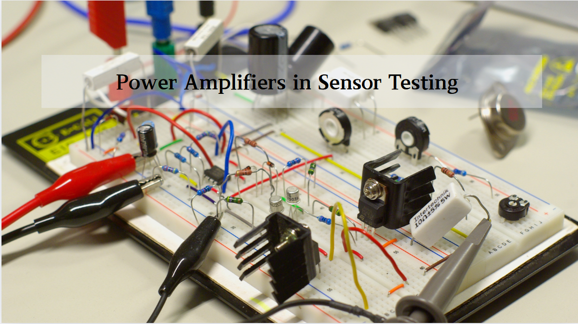
Multivariate Application Analysis of Power Amplifiers in Sensor Testing
In the field of modern sensor testing, power amplifiers (PAs) serve as core components and play an indispensable role. From amplifying weak signals to simulating complex physical environments, power amplifiers provide solid guarantees for the precise testing of sensor performance through their uniqu...
-
2025 / 06 / 28
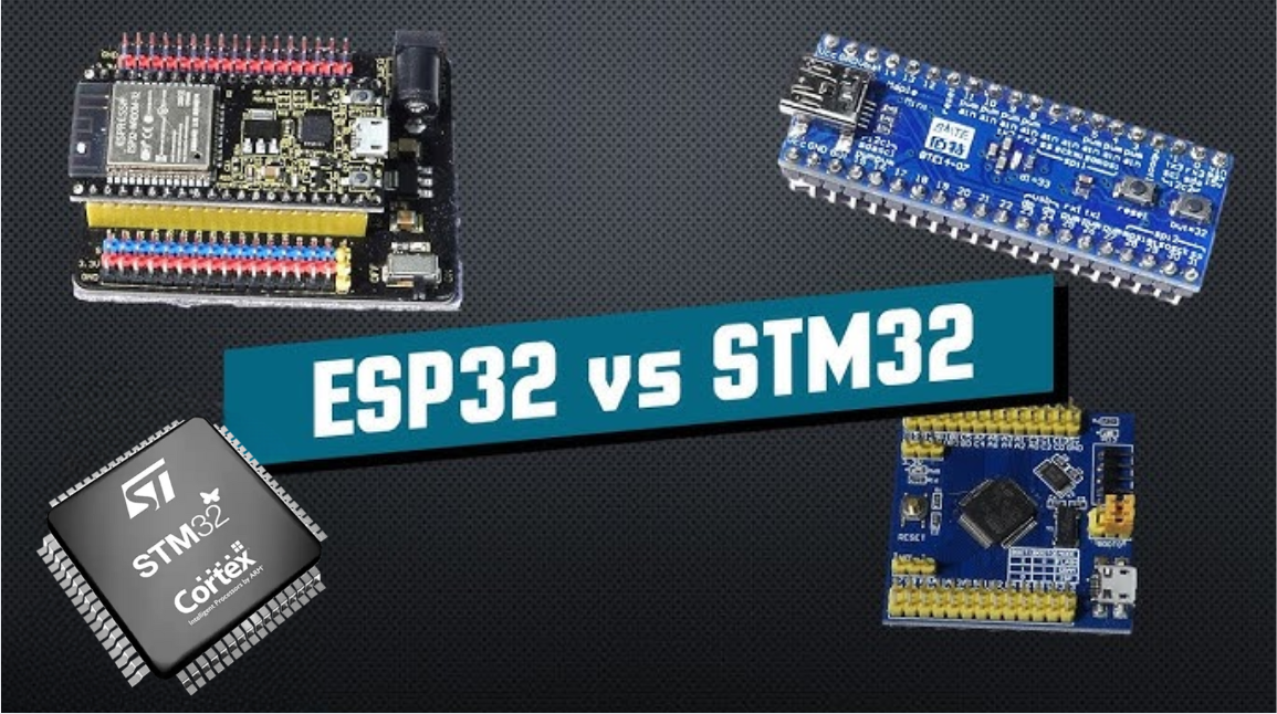
ESP32 vs STM32: Which Microcontroller Suits You Better?
In the field of embedded development, both ESP32 and STM32 are highly favored microcontrollers, each with unique features and advantages. When facing project development, how do you choose between them? This requires comprehensive consideration of multiple factors. The following detailed comparison ...
-
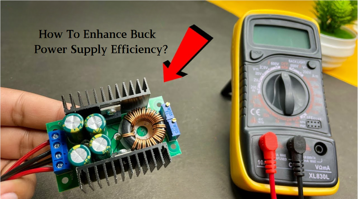
2025 / 06 / 26
Key Strategies to Enhance Buck Power Supply Efficiency
Improving the efficiency of Buck (step-down) switching power supplies requires a multi-dimensional approach targeting energy loss sources, including component selection, topology optimization, control strategies, and thermal management. Below are core strategies and engineering practices:...
-
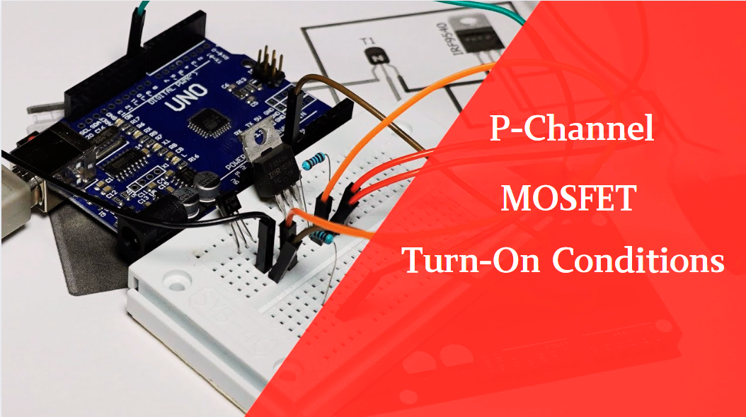
2025 / 06 / 26
P-Channel MOSFET Turn-On Conditions
The turn-on conditions for a P-channel MOSFET (PMOS) are inverse to those of an N-channel MOSFET (NMOS), primarily governed by the relationship between the gate-source voltage (VGS) and the threshold voltage (Vth), along with voltage polarity. Here are the key points:A PMOS turns on when its gate vo...
-
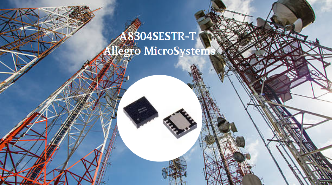
2025 / 06 / 24
A8304SESTR-T Allegro MicroSystems-Single LNB Supply and Control Voltage Regulator
The Allegro MicroSystems A8304SESTR-T is a single-channel Low Noise Block Regulator (LNBR). It integrates a monolithic boost converter with MOSFET, current sensing, and compensation. Featuring a 704 kHz switching frequency, it uses few external components. With an I²C-compatible interface, it offers...
-
2025 / 06 / 20
EG25GGC-128-SGNS by Quectel Wireless Solutions Co., Ltd: Features,Symbol,Footprint and Datasheet
The Quectel EG25GGC - 128 - SGNS is an LTE Cat 4 module optimized for M2M and IoT. Supporting 3GPP Rel. 11, it offers up to 150Mbps downlink and 50Mbps uplink. With global LTE/UMTS/GSM coverage, it's backward - compatible with EDGE/GPRS. Featuring multi - constellation GNSS (GPS, GLONASS, BeiDou, et...


2000+
Daily average RFQ Volume

30,000,000
Standard Product Unit

2800+
Worldwide Manufacturers

15,000 m2
In-stock Warehouse
 Wishlist (0 Items)