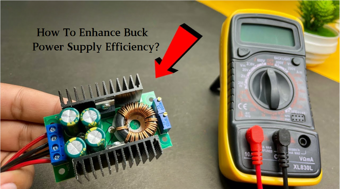
Improving the efficiency of Buck (step-down) switching power supplies requires a multi-dimensional approach targeting energy loss sources, including component selection, topology optimization, control strategies, and thermal management. Below are core strategies and engineering practices:

1. Reducing Switching Losses: Optimizing Dynamic Processes
1.1 High-Speed, Low-Loss Switching Device Selection
MOSFET/GaN Devices:
Choose components with low gate charge (Qg) and output capacitance (Coss), such as TI’s CSD18534Q5B (Qg=6.5nC, ).
For high-frequency applications (>1 MHz), use gallium nitride (GaN) devices (e.g., TI LMG5200), which boost switching speed by 10x and reduce losses by 50%.
Drive Circuit Optimization:
Employ dedicated gate drivers (e.g., TI UCC27211) to compress switching delays from nanoseconds to picoseconds, minimizing voltage-current overlap losses during transitions.
1.2 Soft Switching Techniques
Quasi-Resonant (QR) Topology:
Add a resonant capacitor to the traditional Buck circuit to leverage inductor leakage inductance and MOSFET junction capacitance for zero-voltage switching (ZVS). Suitable for high-voltage applications (e.g., 48V→12V), this improves efficiency by 3%–5%.
Multi-Phase Staggered Control:
Parallel 2-phase or 4-phase Buck converters with 180°/90° phase shifts to reduce input/output ripple current and distribute switching losses. Ideal for high-current scenarios (e.g., server power supplies, TI TPS53631).
2. Minimizing Conduction Losses: Static Parameter Optimization
2.1 Full Replacement of Diodes with Synchronous Rectification
Freewheeling Loss Comparison:
A Schottky diode (0.5V voltage drop) dissipates 2.5W at 5A load, while a synchronous MOSFET () dissipates only 0.25W, improving efficiency by ~8%.
Drive Considerations:
Use controllers with dead-time control (e.g., ADI LTC7820) to prevent shoot-through and optimize light-load efficiency via adaptive on-time.
2.2 Low-Resistance Component Design
Inductor:
Select low-DCR inductors with flat wire winding (e.g., Coilcraft XAL series, DCR < 5mΩ) and magnetic shielding to reduce EMI.
Capacitor:
Parallel multi-layer ceramic capacitors (MLCCs) for output capacitance, with total ESR < 10mΩ. For example, 3×10μF/125℃ X7R capacitors in parallel can handle >6A ripple current.
3. Topology and Control Strategies: Dynamic Efficiency Optimization
3.1 Adaptive Mode Switching
Load-Sensing Control:
Switch to pulse frequency modulation (PFM) at light loads. For example, the TI LM25118 maintains >85% efficiency with <10mA load and a quiescent current as low as 30μA.
Use fixed-frequency PWM for heavy loads to ensure dynamic response (e.g., ripple voltage <1% of output voltage).
3.2 Wide Input Voltage Optimization
Segmented Voltage Regulation:
For wide input ranges (e.g., 4.5V–36V), use a Buck-Buck cascade topology to avoid excessive switching losses from low duty cycles (D < 0.1) in single-stage Buck converters.
Example: A front-end Buck reduces 36V to 12V, and a rear-end Buck further steps down to 5V, improving total efficiency by 6% compared to a single-stage design.
4. Thermal Management and Layout: From Design to Implementation
4.1 Component Thermal Characterization
MOSFET Thermal Design:
Choose low-thermal-resistance packages (e.g., QFN 3x3, ℃) and connect PCB thermal pads directly to metal enclosures to keep junction temperature (Tj) below 100℃.
Inductor Thermal Derating:
Ensure inductor operating current stays below 80% of saturation current (e.g., continuous current ≤8A for a 10A saturation inductor) to avoid efficiency drops from core saturation.
Minimized Power Loop:
Keep the input capacitor→MOSFET→inductor path within 10mm. Use 4-layer PCBs with a full ground plane in the inner layer to reduce loop inductance (<1nH).
Signal-Power Isolation:
Route feedback sampling lines (FB) away from inductor and switch nodes to avoid high-frequency noise coupling; differential sampling can enhance noise immunity.
5. Cutting-Edge Technologies and Case Studies
5.1 Wide-Bandgap Semiconductor Applications
GaN Buck Power Supply:
A TI LMG5200 GaN FET-based design for 24V→3.3V/5A power supply operates at 2MHz, reducing inductor size by 50% and achieving 94% efficiency (vs. ~90% for traditional MOSFETs).
5.2 Magnetic Integration Techniques
Coupled Inductor Solutions:
In multi-phase Buck converters, integrated magnetic core coupled inductors (e.g., 2-phase Buck) improve ripple current cancellation by 30% and reduce core losses by 20%.
6. Efficiency Optimization Verification and Debugging
Key Test Points:
Use an oscilloscope to measure MOSFET Vgs and Vds waveforms, ensuring switching transition times <50ns and minimal ringing (overshoot <10% of supply voltage).
Use an infrared thermal imager to check MOSFET and inductor temperatures, keeping hotspot temperature differences within 10℃ to avoid localized overheating.
Loss Decomposition Method:
Measure no-load losses (dominated by switching losses) with the inductor disconnected, and full-load conduction losses with the inductor connected, to identify and optimize primary loss sources.
Conclusion: A Systems Approach to Efficiency Improvement
High-Frequency + Wide-Bandgap: Suitable for size-sensitive applications (e.g., drone power supplies), trading some switching losses for compact form factors.
Synchronous Rectification + Multi-Phase: Ideal for high-current scenarios (e.g., CPU power supplies), reducing single-device stress through parallel current sharing.
Adaptive Control + Thermal Design: Ensures high efficiency across all load ranges (light load >80%, heavy load >92%) and extends component lifespan via thermal management.
By integrating these strategies, Buck power supply efficiency can reach 92%–95% at typical loads (50%), meeting EMI and temperature rise requirements while providing reliable solutions for high-density power systems.
Hot-selling products of SIC
71421LA55J8 UPD44165184BF5-E40-EQ3-A SST39VF800A-70-4C-B3KE IS66WV1M16DBLL-55BLI-TR AS4C32M16SB-7BIN W25Q16FWSNIG
AS7C34098A-20JIN 752369-581-C W957D6HBCX7I TR IS61LPS12836EC-200B3LI MX25L12875FMI-10G QG82915PL
Product information is from SIC Electronics Limited. If you are interested in the product or need product parameters, you can contact us online at any time or send us an email: sales@sic-chip.com.


 Wishlist (0 Items)