1. Introduction: The "All-Rounder" Quad Op-Amp
In the world of electronic circuits, the LM324 stands as a versatile engineer, serving as a core component across industrial control, consumer electronics, and medical devices through its quad-channel integration, wide voltage adaptability, and cost-effectiveness. This classic op-amp, born in the 1970s, continues to thrive with its compatibility for single-supply 3V~32V (dual-supply ±1.5V~±16V), 1.2MHz bandwidth, and 0.5V/μs slew rate. Whether amplifying microvolt-level sensor signals or converting levels in 5V systems, the LM324 achieves precise control with minimalist circuits.
2. Core Features: The "Rugged" Four-in-One Design
2.1. Hardware Architecture: Four Independent Channels for Flexible Networking
Internally integrated with four fully differential op-amps sharing power supplies (pin 4 for VCC, pin 11 for GND), each channel includes non-inverting (IN+), inverting (IN-) inputs, and a single-ended output (OUT). The differential input stage supports common-mode voltage covering the negative supply rail (down to 0V in single-supply mode), eliminating the need for extra biasing to directly interface with low-level sensors like thermocouples and strain gauges.
2.2. Electrical Robustness: Wide Voltage, Low Power, and Protection
Voltage Adaptability: Single supply from 3V (lithium batteries) to 32V (industrial bus), dual supply from ±1.5V (portable devices) to ±16V (instruments), fitting over 90% of system voltages.
Power Control: Quiescent current of only 375μA per channel, total power consumption <1.5mA for four channels, ideal for battery-powered IoT nodes.
Safety Mechanisms: Output short-circuit protection (sustains continuous shorting), input ESD clamping (±2kV HBM), resilient against PCB soldering errors.
2.3. Performance Parameters: Balancing Practicality and Cost
Parameter | Typical Value | Key Value Proposition |
|---|---|---|
Open-loop Gain | 100dB | Ensures closed-loop accuracy, error <0.1% at 10× gain |
Input Bias Current | 20nA | Suits high-impedance sensors (e.g., pH electrodes) |
Output Swing (5V) | 0.05V~4.8V | Near rail-to-rail, directly drives 5V logic circuits |
Temperature Range | 0℃~70℃ | Covers 90% of civil applications; industrial grade LM224 available |
3. Pin Decoding: The 14-Pin "Universal Socket"
Taking the DIP-14 package as an example, pin functions follow a "3+1" structure (three op-amps + common power supply):
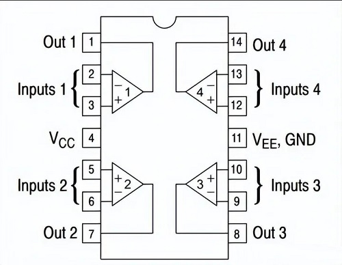
| Pin Number | Pin Name | Description |
|---|---|---|
| 1 | Output 1 | Output of Op-Amp 1 |
| 2 | Input 1- | Inverting input of Op-Amp 1 |
| 3 | Input 1+ | Non-inverting input of Op-Amp 1 |
| 4 | VCC | Positive supply voltage |
| 5 | Input 2+ | Non-inverting input of Op-Amp 2 |
| 6 | Input 2- | Inverting input of Op-Amp 2 |
| 7 | Output 2 | Output of Op-Amp 2 |
| 8 | Output 3 | Output of Op-Amp 3 |
| 9 | Input 3- | Inverting input of Op-Amp 3 |
| 10 | Input 3+ | Non-inverting input of Op-Amp 3 |
| 11 | Vee/GND | Ground or negative supply voltage |
| 12 | Input 4+ | Non-inverting input of Op-Amp 4 |
| 13 | Input 4- | Inverting input of Op-Amp 4 |
| 14 | Output 4 | Output of Op-Amp 4 |
Pin No. | Symbol | Function Definition | Typical Application Scenarios |
|---|---|---|---|
1/7/8/14 | OUT1-4 | Four push-pull outputs, 40mA sink current per channel | Drive LEDs, relays, or ADC sample-and-hold |
2/6/9/13 | IN- | Inverting input (virtual ground node) | Connect feedback resistors to determine closed-loop gain |
3/5/10/12 | IN+ | Non-inverting input (high-Z signal port) | Directly connect to sensors or voltage dividers |
4 | VCC | Positive supply (single/dual supply) | Connect to system power, recommend 100nF decoupling |
11 | GND | Ground/negative supply (dual supply) | Full-circuit reference ground, require single-point grounding |
Layout Tips: Avoid parallel routing of IN+ and IN- pins for adjacent op-amps to reduce crosstalk; thicken VCC and GND traces to mitigate power noise.
4. Working Principle: The "Assembly Line" Philosophy of Three-Stage Amplification
Each op-amp employs a classic three-stage architecture, analogous to a precision production line:
Differential Input Stage: Bipolar transistor differential pair amplifies Vin+ - Vin- signals with 80dB CMRR, filtering out 50Hz mains interference.
Intermediate Gain Stage: Common-emitter amplifier with frequency compensation, integrated 10pF capacitor prevents self-oscillation above 1MHz for closed-loop stability.
Push-Pull Output Stage: Class AB amplifier structure, output resistance <100Ω, drives 10kΩ loads, limits current to 50mA during short circuits.
5. Five Classic Applications: From Signal Chain to Power Chain
5.1. Sensor Conditioning: Thermocouple Cold Junction Compensation
Circuit: Op-amp configured as non-inverting amplifier (gain 100), IN+ connects to thermocouple (mV signals), IN- grounds via 10kΩ resistor, feedback resistor 1MΩ.
Key: Leverages IN+ common-mode-to-GND characteristic to amplify 0~20mV temperature differences without biasing, suitable for Type K thermocouples.
Optimization: 100kΩ parallel resistor at input prevents op-amp saturation during thermocouple open-circuit.
5.2. Single-Supply Audio Amplification: 3V Microphone Preamplifier
Inverting Circuit: Ri=1kΩ (matches electret mic impedance), Rf=10kΩ (gain -10), 1/2VCC biasing via two 10kΩ voltage dividers.
Tip: 10μF output capacitor blocks DC, reduces 50Hz ripple, THD <1% (1kHz sine wave).
Expansion: Four op-amps can cascade into two-stage filters for 20Hz~20kHz audio channels.
5.3. Voltage Comparator: Lithium Battery Overvoltage Protection
Window Detection: Two op-amps set thresholds at 4.2V (charge cutoff) and 2.5V (discharge cutoff); when battery voltage exits [2.5V, 4.2V], low output triggers MOSFET shutdown.
Innovation: Utilizes op-amp push-pull output to drive NPN transistors directly, eliminating pull-up resistors and reducing circuit cost by 30%.
5.4. Integrator Circuit: Motor Speed Monitoring
Principle: Hall sensor square waves pass through RC integration (R=100kΩ, C=10μF), op-amp as integrator; output voltage proportional to speed (0~5V for 0~5000rpm).
Calibration: Potentiometer adjusts feedback resistor to compensate for component errors, linearity ±0.5%.
5.5. Oscillator: A "Drop-in" Alternative to 555
Square Wave Generation: Op-amp configured as Schmitt trigger, RC time constant from 100kΩ resistor and 10nF capacitor (frequency ≈1kHz), 50% duty cycle.
Advantage: Eliminates 555’s dual-comparator structure, achieves with single op-amp + passives, reduces PCB area by 40%.
6. LM324 Typical Application Circuits
1. LM324 as an Inverting AC Amplifier
This amplifier replaces transistors for AC amplification, suitable for pre-amplification in sound systems. The circuit requires no adjustment, using a single power supply where R1 and R2 form a 1/2V+ bias. C1 acts as a damping capacitor.
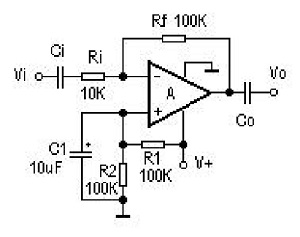
The voltage gain (AV) is determined by external resistors RI and RF: AV=−RF/RI
The negative sign indicates the output signal is inverted relative to the input. For values shown, AV = -10. The input resistance equals RI, typically matched to the signal source's internal resistance, with RF selected for the desired gain. CO and CI are coupling capacitors.
This circuit features high input impedance. R1 and R2 form a 1/2V+ voltage divider, biasing the op-amp via R3.
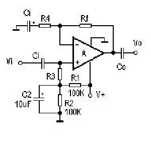
The voltage gain formula is:AV=1+RF/R4
Input resistance is set by R3, with R4 typically ranging from several kΩ to tens of kΩ.
The temperature probe uses a silicon transistor (3DG6) configured as a diode. The transistor's base-emitter voltage has a temperature coefficient of -2.5mV/°C, meaning it decreases by 2.5mV for each °C increase. Op-amp A1 acts as a non-inverting DC amplifier: higher temperatures reduce the voltage drop across BG1, lowering the voltage at A1's non-inverting input and its output.
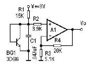
This is a linear amplification process. Connecting a measurement or control circuit to A1's output enables indication or automatic control.
Removing the feedback resistor (or treating it as infinite) places the op-amp in an open-loop condition. Though theoretically infinite, LM324's open-loop gain is 100dB (100,000×), making it a voltage comparator with outputs at high (V+) or low (V- or GND) levels. The output is low when the positive input voltage exceeds the negative input.
Two op-amps form a voltage level comparator:
R1 and R1' set the comparison threshold U1 for A1.
R2 and R2' set threshold U2 for A2.
Input voltage UI connects to A1's positive input and A2's negative input.
If UI > U1, A1 outputs high.
If UI < U2, A2 outputs high.
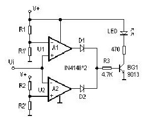
Either high output turns on transistor BG1, lighting the LED.
With U1 > U2, the LED lights when UI exits [U2, U1], acting as a voltage level indicator.
With U2 > U1, the LED lights when UI is within [U2, U1], serving as a "window" voltage indicator.
Modified for use with sensors, this circuit detects dual limits for physical quantities, short circuits, open circuits, etc.
7. Selection and Alternatives: Scenario-Driven Choices
Application Scenario | Recommended Model | Alternative | Key Difference |
|---|---|---|---|
Low-Cost Prototyping | Quad-channel saves 30% PCB space | ||
Industrial Environments | SGM324 (domestic Chinese) | Wide temp range + 4kV ESD for outdoor use | |
Battery-Powered Devices | Quiescent current 110μA, extends battery life by 50% | ||
Digital Interfaces | No direct substitute | Requires pull-up resistors for 5V logic |
9. LM324 Package 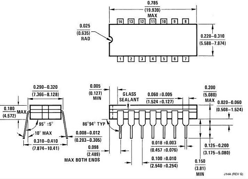

10.Conclusion: LM324, an Evergreen Classic
From 1970s calculators to 2020s smart homes, the LM324 has proven over half a century that true classics lie in solving complex problems with the simplest architectures. Its charm stems not only from quad-channel space savings but also from its deep understanding of single-supply systems—when 90% of applications need only 5V, the LM324 has ingrained the philosophy of "no dual supplies needed" into its DNA. For engineers, the LM324 is more than a component; it’s a design philosophy: achieving the most reliable functions with the fewest external parts. In the foreseeable future, this "four-in-one" op-amp will continue to script simple yet powerful electronic narratives at every node of the signal chain.
Hot-selling products of SIC
71421LA55J8 UPD44165184BF5-E40-EQ3-A SST39VF800A-70-4C-B3KE IS66WV1M16DBLL-55BLI-TR AS4C32M16SB-7BIN W25Q16FWSNIG
AS7C34098A-20JIN 752369-581-C W957D6HBCX7I TR IS61LPS12836EC-200B3LI MX25L12875FMI-10G QG82915PL
Product information is from SIC Electronics Limited. If you are interested in the product or need product parameters, you can contact us online at any time or send us an email: sales@sic-chip.com.




 Wishlist (0 Items)