

- RFQ
- BOM
-
Contact Us
Tel: +86-0755-83501315
Email: sales@sic-components.com


- Chinese
- English
- French
- German
- Portuguese
- Spanish
- Russian
- Japanese
- Korean
- Arabic
- Irish
- Greek
- Turkish
- Italian
- Danish
- Romanian
- Indonesian
- Czech
- Afrikaans
- Swedish
- Polish
- Basque
- Catalan
- Esperanto
- Hindi
- Lao
- Albanian
- Amharic
- Armenian
- Azerbaijani
- Belarusian
- Bengali
- Bosnian
- Bulgarian
- Cebuano
- Chichewa
- Corsican
- Croatian
- Dutch
- Estonian
- Filipino
- Finnish
- Frisian
- Galician
- Georgian
- Gujarati
- Haitian
- Hausa
- Hawaiian
- Hebrew
- Hmong
- Hungarian
- Icelandic
- Igbo
- Javanese
- Kannada
- Kazakh
- Khmer
- Kurdish
- Kyrgyz
- Latin
- Latvian
- Lithuanian
- Luxembou..
- Macedonian
- Malagasy
- Malay
- Malayalam
- Maltese
- Maori
- Marathi
- Mongolian
- Burmese
- Nepali
- Norwegian
- Pashto
- Persian
- Punjabi
- Serbian
- Sesotho
- Sinhala
- Slovak
- Slovenian
- Somali
- Samoan
- Scots Gaelic
- Shona
- Sindhi
- Sundanese
- Swahili
- Tajik
- Tamil
- Telugu
- Thai
- Ukrainian
- Urdu
- Uzbek
- Vietnamese
- Welsh
- Xhosa
- Yiddish
- Yoruba
- Zulu
- Kinyarwanda
- Tatar
- Oriya
- Turkmen
- Uyghur
- Tag List
- High-Voltage Analog Switch ICs: Technical Principles, Core Characteristics, and Comprehensive Application Analysis
High-Voltage Analog Switch ICs: Technical Principles, Core Characteristics, and Comprehensive Application Analysis
I. Technical Definition and Evolution Background of High-Voltage Analog Switch ICs https://www.sic-components.com/analog-switches-multiplexers-demultiplexers
High-Voltage Analog Switch ICs refer to solid-state switching devices capable of handling analog signals with peak voltages exceeding ±100V. Their core function is to achieve signal conduction, isolation, and routing in high-voltage environments. Compared with traditional mechanical relays, these ICs feature nanosecond-level switching speed, micrometer-scale package size, and a service life of over one million switching cycles, fundamentally revolutionizing high-voltage signal processing.
The technological evolution of high-voltage analog switch ICs has gone through three stages:
Silicon-based MOSFET Era (1980–2000): Based on complementary P/N channel MOSFET structures, with typical voltage resistance of ±200V (e.g., TI's TS3011).
SOI Process Breakthrough (2000–2010): Silicon-On-Insulator (SOI) technology realizes electrical isolation between devices and the substrate, increasing voltage resistance to ±600V (e.g., Littelfuse's CPC7500 series).
Wide Bandgap Material Application (2010–Present): Silicon Carbide (SiC) and Gallium Nitride (GaN) materials enable devices to maintain low on-resistance (RDS(on) < 10mΩ) under 1200V high voltage (e.g., Power Integrations' InnoMux™-2 series).
II. Analysis of Core Working Principles and Physical Structure
2.1 Underlying Realization Mechanism of High-Voltage Switches
The conduction and cutoff of high-voltage analog switch ICs rely on the field effect of MOSFETs. Take a ±320V device as an example:
Conduction State: When a positive voltage (e.g., +5V) is applied to the gate, both P-channel and N-channel MOSFETs conduct, forming a low-resistance path from input to output, with typical RDS(on) = 14.5Ω (Littelfuse CPC7514).
Cutoff State: When the gate voltage is zero, the MOSFET channel disappears. Parasitic capacitance (e.g., CISS = 50pF) and the oxide layer (thickness > 20nm) together form a high-voltage barrier, achieving a cutoff impedance > 10⁹Ω.
2.2 Key Structural Design Technologies
(1) SOI Isolation Layer Technology
Principle: A 2μm-thick silicon dioxide insulating layer is grown on the silicon substrate to completely isolate high-voltage devices from the substrate, avoiding latch-up effects.
Advantage: Enables isolation between adjacent switch channels to reach 110dB@5kHz (Littelfuse CPC7560), far higher than the 60dB of traditional silicon processes.
(2) RESURF Voltage-Resistant Structure
Design: Gradient doping is introduced into the N-type drift region to homogenize the electric field distribution, increasing the breakdown voltage to over 600V.
Application: STMicroelectronics' STHV64SW adopts this structure, maintaining RDS(on) = 29Ω under ±200V.
III. Core Performance Parameters and Technical Characteristics
3.1 Electrical Characteristics Matrix
Parameter Category Typical Indicators Technical Impact
Voltage Resistance Range ±320V (Littelfuse)/±600V (CPC7560) Determines the upper voltage limit of application scenarios
On-Resistance RDS(on) 4Ω@±100V (ABLIC)/12.5Ω@±90V (MP4816) Directly affects signal attenuation and power consumption (P = I²×R)
Off Isolation -60dB@1kHz/-110dB@5kHz (Littelfuse) Prevents channel crosstalk and ensures multi-channel operation
Switching Speed tON = 100ns/tOFF = 80ns (STHV64SW) Determines high-frequency signal processing capability (e.g., ultrasonic probe pulses)
Parasitic Capacitance CDS = 15pF (ABLIC) Limits bandwidth (BW = 1/(2π×R×C))
3.2 Advanced Technical Features
(1) Single-Supply Driving Technology
Breakthrough: ABLIC's high-voltage switches can drive ±100V signals with a single 5V power supply, eliminating the need for positive/negative dual supplies.
Application: In portable medical devices, it saves 50% of the power module volume.
(2) Intelligent Protection Integration
Function: STHV64SW integrates over-temperature shutdown (150°C threshold) and under-voltage lockout (UVLO), increasing reliability by 30% in industrial environments.
Mechanism: When the junction temperature exceeds the threshold, the built-in thermistor triggers the logic circuit to force all channels off.
IV. Typical Application Scenarios and Solutions
4.1 Medical Ultrasound Imaging Systems
Pain Points
Probes require ±90V high-voltage pulses to excite piezoelectric crystals, while channel crosstalk must be < -80dB.
Traditional solutions require positive/negative high-voltage supplies, leading to large system size and high power consumption.
Innovative Solutions
Device Selection: Monolithic Power Systems' MP4816 (16 channels, ±90V voltage resistance).
Technical Advantages:
Eliminates positive/negative supplies, directly powered by a +180V single supply, reducing power design complexity by 40%.
Integrates output bleed resistors to avoid probe aftershock interference, improving image resolution by 15%.
4.2 Industrial High-Voltage Testing Equipment
Scene Challenges
Testing voltages up to ±300V, signal frequency 20MHz, requiring switch loss < 0.5W.
Traditional relays have slow switching speed (ms level), failing to meet high-frequency testing needs.
Solutions
Device Combination: Littelfuse CPC7532 (±320V, 14.5Ω) + impedance matching network.
Performance Improvements:
Switching speed of 100ns supports distortion-free transmission of 20MHz signals.
Channel isolation > 100dB during multi-channel parallel testing, improving testing accuracy to ±0.1%.
4.3 New Energy Vehicle Battery Management
Core Requirements
Battery pack voltage reaches 400V, requiring high-voltage switches for charge/discharge circuit control.
Low-power design with standby current < 1μA.
Technical Breakthroughs
Wide Bandgap Solution: Power Integrations' InnoMux™-2 (1700V GaN switch).
Key Indicators:
RDS(on) = 8mΩ, reducing conduction loss by 70% compared to silicon devices.
Supports 100kHz high-frequency switching, reducing the volume of on-board chargers by 50%.
V. Selection Guide and Design Key Points
5.1 Core Parameter Decision Tree
(1) Voltage Range Determination
Working voltage ×1.5 ≤ device voltage resistance (e.g., select ±600V devices for 400V battery systems).
Consider surge factors: Automotive applications require an additional 30% margin (cold start pulses can reach 600V).
(2) Power Consumption Budget Calculation
Conduction power: Pd_ON = I²×RDS(on) (e.g., 5A current through 10mΩ resistance generates 0.25W power consumption).
Switching power: Pd_SW = QG×V×f (QG = 20nC, V = 300V, f = 10kHz results in 0.6W power consumption).
Heat sinks (RθJA < 50°C/W) are required when total power > 1W.
(3) Signal Integrity Design
High-frequency scenarios (>10MHz): Series 100Ω/100MHz beads to suppress ringing.
Long trace applications: Parallel 100nF ceramic capacitors at the switch output to compensate for parasitic inductance.
VI. Technical Development Trends and Future Prospects
6.1 Material and Process Innovations
Popularization of third-generation semiconductors: SiC MOSFETs will achieve RDS(on) < 5mΩ for 1200V devices by 2025, applied in photovoltaic inverters.
3D integration technology: Integrates drive circuits and high-voltage switches on the same chip (e.g., TI's DRV3205), reducing drive delay from 50ns to 10ns.
6.2 Intelligence and Functional Integration
Built-in diagnostic functions: Future devices will integrate current detection (accuracy ±1%) and fault logging (supporting 100 event logs).
Digital interface upgrades: Support I2C/SPI remote configuration (e.g., future versions of STHV64SW will add PWM dimming functions).
VII. Conclusion
As a bridge connecting high-voltage signals and precision circuits, high-voltage analog switch ICs have directly promoted innovation in medical, industrial, and new energy fields through technological advancements. From the evolution of silicon-based to wide bandgap materials, and from single switches to intelligent integration, these devices are rapidly iterating toward the direction of "high voltage resistance, low loss, and intelligence." In practical applications, engineers must accurately match device parameters according to the voltage, frequency, and power consumption requirements of specific scenarios, and fully unleash the technical potential of high-voltage analog switch ICs through reasonable thermal management and signal chain design, laying the foundation for the next generation of high-voltage electronic systems.
https://www.sic-components.com/analog-switches-multiplexers-demultiplexers


Hot Products
View More-
89810007 Crouzet
-

82334852 Crouzet
-
3RE41227CA114DY0 Siemens
-
R88A-CA1F040B Omron Automation and Safety
-
6SL32201YH280UP0 Siemens
-
3RE41227CA311FF6 Siemens
-
3RW52452AC04 Siemens
-
EADT-E-U1-110 Festo Corporation
-
TMCM-1633-CANOPEN Trinamic Motion Control GmbH
-
17HUG92BF14 Siemens
-
DSML-0630-24E Delta Electronics
-
82802013 Crouzet
Related Blogs
-
2025 / 07 / 04
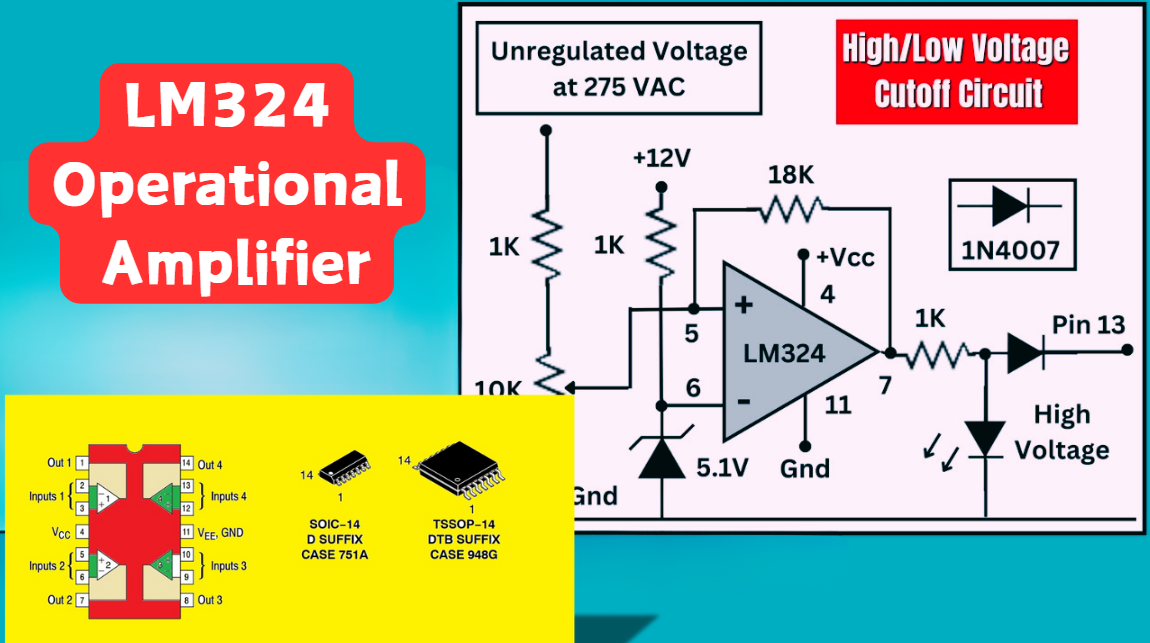
LM324 Operational Amplifier Comprehensive Guide: Pins, Applications, Packaging, and Datasheet
The LM324 is a low-cost integrated circuit featuring four independent operational amplifiers (op-amps), renowned for its wide voltage adaptability, low power consumption, and high reliability in industrial and consumer electronics. With a single-supply voltage range of 3V to 32V (or dual-supply rang...
-
2025 / 07 / 02
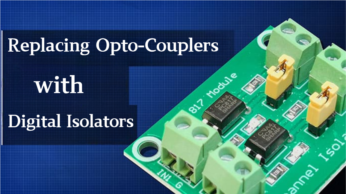
A Comprehensive Guide to Replacing Opto-Couplers with Digital Isolators: From Principles to Practice
In the ever-evolving landscape of electronic design, the transition from opto-couplers to digital isolators marks a pivotal shift in isolation technology. For decades, opto-couplers have been the cornerstone of electrical isolation in industrial control, medical devices, and power systems, relying o...
-
2025 / 06 / 30
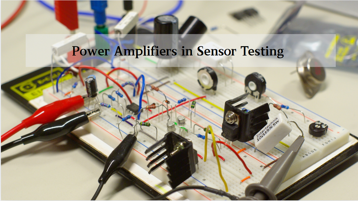
Multivariate Application Analysis of Power Amplifiers in Sensor Testing
In the field of modern sensor testing, power amplifiers (PAs) serve as core components and play an indispensable role. From amplifying weak signals to simulating complex physical environments, power amplifiers provide solid guarantees for the precise testing of sensor performance through their uniqu...
-
2025 / 06 / 28
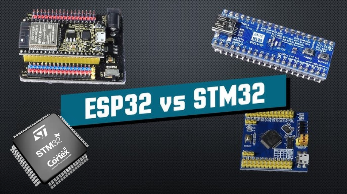
ESP32 vs STM32: Which Microcontroller Suits You Better?
In the field of embedded development, both ESP32 and STM32 are highly favored microcontrollers, each with unique features and advantages. When facing project development, how do you choose between them? This requires comprehensive consideration of multiple factors. The following detailed comparison ...
-
2025 / 06 / 26
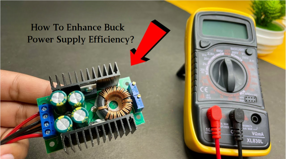
Key Strategies to Enhance Buck Power Supply Efficiency
Improving the efficiency of Buck (step-down) switching power supplies requires a multi-dimensional approach targeting energy loss sources, including component selection, topology optimization, control strategies, and thermal management. Below are core strategies and engineering practices:...
-
2025 / 06 / 26
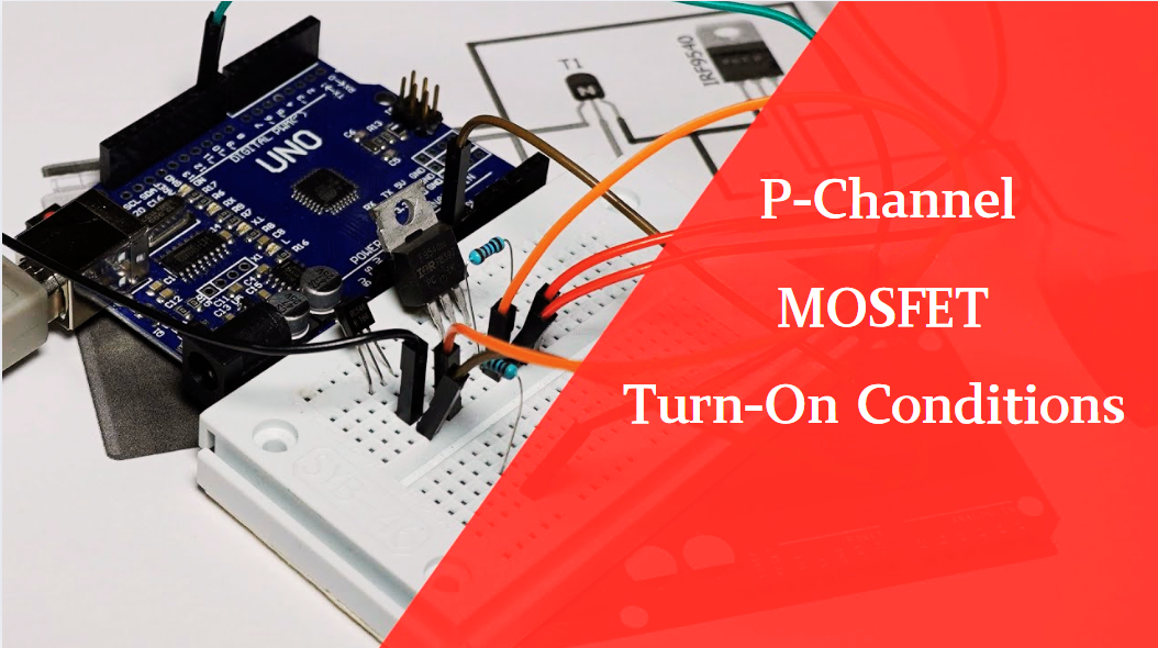
P-Channel MOSFET Turn-On Conditions
The turn-on conditions for a P-channel MOSFET (PMOS) are inverse to those of an N-channel MOSFET (NMOS), primarily governed by the relationship between the gate-source voltage (VGS) and the threshold voltage (Vth), along with voltage polarity. Here are the key points:A PMOS turns on when its gate vo...
-
2025 / 06 / 24
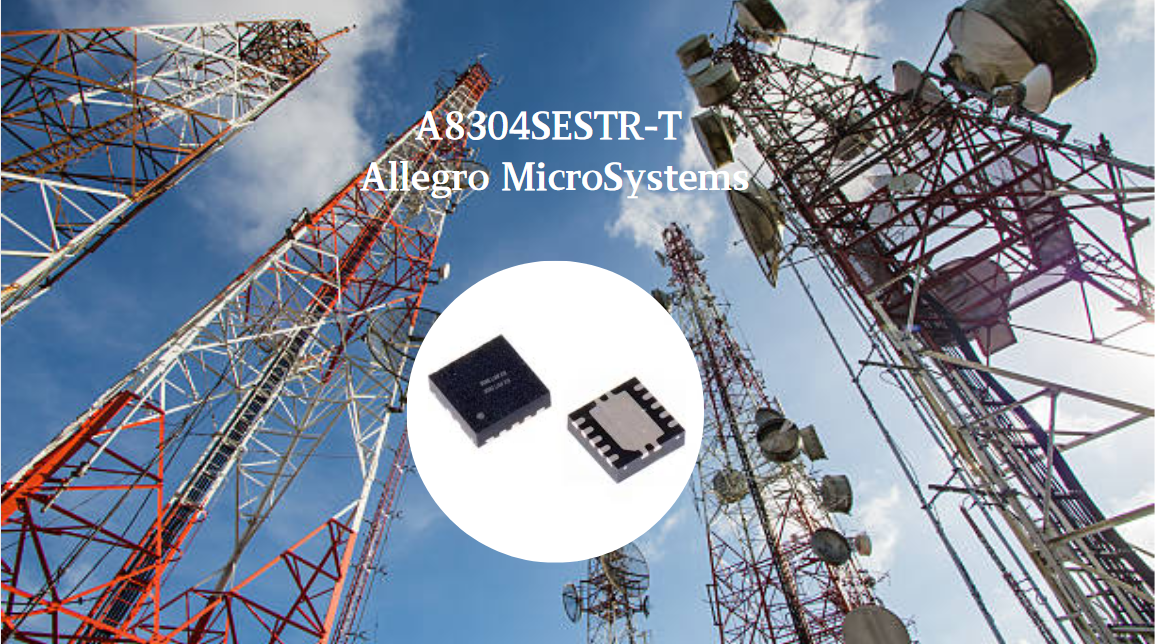
A8304SESTR-T Allegro MicroSystems-Single LNB Supply and Control Voltage Regulator
The Allegro MicroSystems A8304SESTR-T is a single-channel Low Noise Block Regulator (LNBR). It integrates a monolithic boost converter with MOSFET, current sensing, and compensation. Featuring a 704 kHz switching frequency, it uses few external components. With an I²C-compatible interface, it offers...
-
2025 / 06 / 20
EG25GGC-128-SGNS by Quectel Wireless Solutions Co., Ltd: Features,Symbol,Footprint and Datasheet
The Quectel EG25GGC - 128 - SGNS is an LTE Cat 4 module optimized for M2M and IoT. Supporting 3GPP Rel. 11, it offers up to 150Mbps downlink and 50Mbps uplink. With global LTE/UMTS/GSM coverage, it's backward - compatible with EDGE/GPRS. Featuring multi - constellation GNSS (GPS, GLONASS, BeiDou, et...

-
2025 / 06 / 17
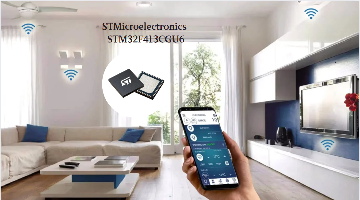
STMicroelectronics STM32F413CGU6 Microcontroller: Datasheet, Performance, Features
The STMicroelectronics STM32F413CGU6 is an Arm® Cortex®-M4 based MCU with FPU, operating at up to 100 MHz for 125 DMIPS performance. It features 1MB Flash, 320KB SRAM, and interfaces like USB OTG FS, 3 CAN, ADC, 2 DAC, and multiple serial ports. With low-power modes (Sleep, Stop, Standby), it suits ...
-
2025 / 06 / 13
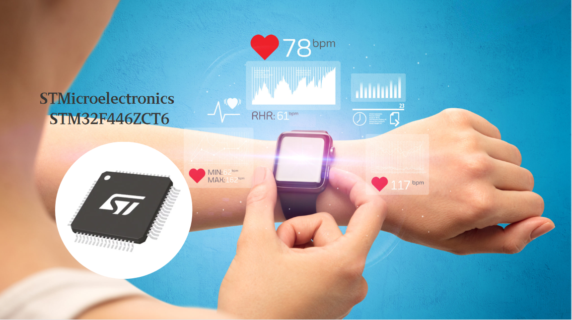
STMicroelectronics STM32F446ZCT6 -Microcontrollers: A Comprehensive Guide
The STMicroelectronics STM32F446ZCT6 is an ARM Cortex-M4-based MCU with FPU, running at up to 180 MHz. It features 256 KB Flash, 128 KB SRAM + 4 KB backup SRAM, and offers rich peripherals: USB OTG HS/FS, 2 CAN, 3 ADCs, 17 timers, and 20 communication interfaces. In LQFP144 package, industrial temp ...

2000+
Daily average RFQ Volume

30,000,000
Standard Product Unit

2800+
Worldwide Manufacturers

15,000 m2
In-stock Warehouse
 Wishlist (0 Items)