

- RFQ
- BOM
-
Contact Us
Tel: +86-0755-83501315
Email: sales@sic-components.com


- Chinese
- English
- French
- German
- Portuguese
- Spanish
- Russian
- Japanese
- Korean
- Arabic
- Irish
- Greek
- Turkish
- Italian
- Danish
- Romanian
- Indonesian
- Czech
- Afrikaans
- Swedish
- Polish
- Basque
- Catalan
- Esperanto
- Hindi
- Lao
- Albanian
- Amharic
- Armenian
- Azerbaijani
- Belarusian
- Bengali
- Bosnian
- Bulgarian
- Cebuano
- Chichewa
- Corsican
- Croatian
- Dutch
- Estonian
- Filipino
- Finnish
- Frisian
- Galician
- Georgian
- Gujarati
- Haitian
- Hausa
- Hawaiian
- Hebrew
- Hmong
- Hungarian
- Icelandic
- Igbo
- Javanese
- Kannada
- Kazakh
- Khmer
- Kurdish
- Kyrgyz
- Latin
- Latvian
- Lithuanian
- Luxembou..
- Macedonian
- Malagasy
- Malay
- Malayalam
- Maltese
- Maori
- Marathi
- Mongolian
- Burmese
- Nepali
- Norwegian
- Pashto
- Persian
- Punjabi
- Serbian
- Sesotho
- Sinhala
- Slovak
- Slovenian
- Somali
- Samoan
- Scots Gaelic
- Shona
- Sindhi
- Sundanese
- Swahili
- Tajik
- Tamil
- Telugu
- Thai
- Ukrainian
- Urdu
- Uzbek
- Vietnamese
- Welsh
- Xhosa
- Yiddish
- Yoruba
- Zulu
- Kinyarwanda
- Tatar
- Oriya
- Turkmen
- Uyghur
Wide Bandwidth Operational Amplifier
1. Core Definition and Value of Wide-Bandwidth Op Amps
A Wide-Bandwidth Operational Amplifier (Op Amp) is an analog integrated circuit that maintains stable gain across a frequency range from tens of MHz to several GHz, with a core specification Gain-Bandwidth Product (GBW) typically exceeding 50 MHz. Compared to traditional Op Amps, it achieves distortion-free signal amplification from audio to microwave bands through optimized input stage structures, reduced parasitic parameters, and innovative processes, making it a core component in high-speed data acquisition, optical communications, radar detection, and other fields. For example, TI’s OPA656 with a 500 MHz unity-gain bandwidth achieves a 1 MHz transimpedance bandwidth (1 MΩ gain + 47 pF capacitive load) in photodiode amplification, while GaN-process Op Amps push bandwidth beyond 2 GHz, driving the miniaturization of 5G communication modules. (https://www.sic-components.com/amplifiers)
2. Key Technical Characteristics and Classification
2.1 Three Core Parameters
Gain-Bandwidth Product (GBW)
Determines the frequency response capability. For example, Microchip’s MCP6241 with a 550 kHz GBW matches 50 μA low power consumption, suitable for battery-powered devices; TI’s OPA2892 with a 2 GHz GBW and 0.95 nV/√Hz noise meets high-precision testing requirements.
Slew Rate (SR)
Impacts large-signal response speed. OPA680’s 220 V/μs slew rate makes it ideal for video line driving, capable of handling step signals above 200 MHz.
Input Stage Types
FET Input: High input impedance (e.g., MC4558’s gate-controlled PMOS with impedance > 10¹²Ω), suitable for high-impedance signal sources.
Bipolar Input: Low voltage noise (OPA2891’s 0.95 nV/√Hz), suitable for precision measurements.
CMOS Hybrid: Balances power consumption and bandwidth (MCP6241’s 1.8V–5.5V wide voltage range with 50 μA quiescent current).
2.2 Topological Innovations
Voltage Feedback Amplifier (VFA)
Traditional architecture suitable for medium-low gain (<100 V/V), such as OPA656 optimizing linearity via negative feedback in ADC buffering.
Current Feedback Amplifier (CFA)
Breaks the linear relationship between GBW and gain; THS3470 drives 1A loads with 100 MHz bandwidth for high-speed current monitoring.
Quasi-Resonant Compensation
Extends bandwidth via internal RC networks; MC4558 achieves 5.5 MHz unity-gain bandwidth (3x traditional 1458) while maintaining 68° phase margin.
3. Design Practices: Four Key Steps from Selection to Implementation
3.1 Application-Driven Selection
Scenario Requirements Typical Device Design Focus
ADC Buffering Low noise + wide bandwidth OPA656 (500 MHz) Match input impedance with ADC sampling cap
Photodiode Amplification Transimpedance stability + low bias current OPA680 (220 MHz@G=2) Compensation cap to suppress high-frequency oscillation
Portable Devices Low power + rail-to-rail MCP6241 (550 kHz) Noise optimization under 1.8V single supply
Industrial Test Frontends High linearity + noise rejection TI OPA838 (300 MHz) Differential sampling to reduce common-mode noise
3.2 Bandwidth Extension Techniques
Multi-Stage Cascading
Overlapping bandwidth design; two 200 MHz Op Amps cascaded achieve 350 MHz -3dB bandwidth (sacrificing 10% gain flatness).
Negative Feedback Optimization
Reduce closed-loop gain via T-network; MC4558 extends bandwidth to 550 kHz at G=10 (1/10 of open-loop 5.5 MHz).
Impedance Matching
Use π-type LC networks for 50Ω input/output matching at 1 GHz, as in TI’s high-speed current monitoring reference design.
3.3 PCB Layout Best Practices
Minimized Signal Paths
Keep input-to-Op Amp trace length <5 mm to reduce parasitic capacitance (≈0.3 pF per 1 mm trace).
Power Decoupling
Parallel 10 μF tantalum cap + 100 nF ceramic cap at VCC pin, extending cutoff frequency to 100 MHz.
Ground Stratification
Single-point connection between analog and digital grounds to avoid 10–100 MHz noise coupling via ground loops.
3.4 Noise and Stability Balance
Noise Decomposition
In photodiode applications, OPA656’s 7 nV/√Hz voltage noise + 2.5 fA/√Hz current noise results in 12 nV/√Hz equivalent input noise at 1 MΩ transimpedance.
Phase Margin Design
For a 500 MHz GBW Op Amp at G=2, reserve 45° phase margin to avoid oscillations from capacitive loads (>20 pF).
4. Typical Applications and Emerging Trends
4.1 Scenario-Based Applications
Optical Communication Receivers
OPA656 drives 100 MHz photodiodes with 100 pF compensation, achieving 80 MHz -3dB bandwidth and BER <1e-12.
Battery Management Systems (BMS)
TI TLV2365 monitors millivolt-level voltage changes at 50 MHz with <10 μs response time, supporting 200 kHz fast charging.
Medical Imaging
OPA2892 amplifies ultrasonic echo signals at 2 GHz with THD <0.0003%, enhancing B-scan image resolution.
4.2 Technological Evolution
Wide-Bandgap Processes
GaN FET input Op Amps (e.g., TI LMG series) push bandwidth to 8 GHz while reducing switching losses by 50%.
Intelligent Compensation
Adaptive feedback technologies (e.g., ADI’s Σ-Δ compensation) auto-calibrate temperature drift, limiting gain deviation to <0.1% at 125°C.
On-Chip Integration
TI’s THS4521 integrates limiters and Op Amps for 1 GHz signal conditioning, saving 50% board space.
5. Selection and Testing Recommendations
Dynamic Testing
Use network analyzers to measure closed-loop frequency response, focusing on -3dB bandwidth, group delay (<10 ns), and gain flatness (±0.5 dB).
Load Simulation
Parallel 20 pF cap + 1 kΩ resistor at the output to simulate real capacitive loads and verify stability.
Thermal Design Validation
Monitor junction temperature with infrared thermography, ensuring <15% GBW degradation at 125°C (refer to MCP6241’s -40°C to +125°C specifications).
Conclusion
Designing wide-bandwidth Op Amps fundamentally balances bandwidth, noise, and power consumption. From early MC4558 introducing MOSFET inputs to today’s GaN Op Amps breaking GHz barriers, each bandwidth leap drives electronic system innovation. With surging demands in 6G communications, autonomous driving (24–77 GHz radar), and quantum computing (μV-level signal amplification), wide-bandwidth Op Amps will continue evolving toward higher bandwidth (>10 GHz), lower noise (<1 nV/√Hz), and smarter compensation (AI-assisted calibration), serving as critical links between the physical world and digital signals.
https://www.sic-components.com/amplifiers


Hot Products
View More-
C146P06002G8 Amphenol Tuchel Industrial
-
09110009972 HARTING
-
09140100303XL HARTING
-
09405249901 HARTING
-

1108783-2 TE Connectivity AMP Connectors
-
09400169925 HARTING
-
T2070104001-000 TE Connectivity AMP Connectors
-
C146S06005G8 Amphenol Tuchel Industrial
-

09400009955 HARTING
-
1417403 Phoenix Contact
-
1758460000 Weidmüller
-
09110009936 HARTING
Related Blogs
-
2025 / 06 / 30
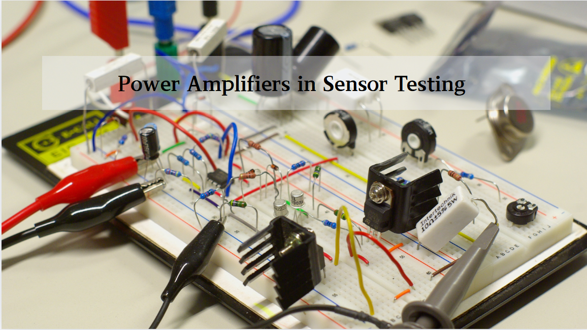
Multivariate Application Analysis of Power Amplifiers in Sensor Testing
In the field of modern sensor testing, power amplifiers (PAs) serve as core components and play an indispensable role. From amplifying weak signals to simulating complex physical environments, power amplifiers provide solid guarantees for the precise testing of sensor performance through their uniqu...
-
2025 / 06 / 28
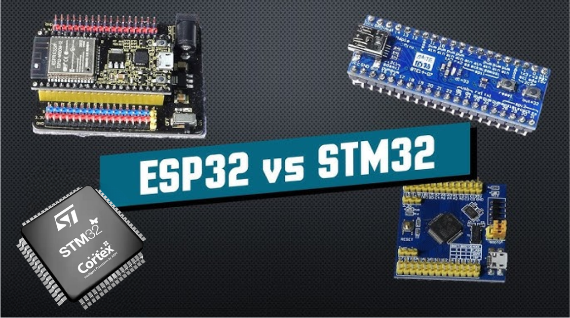
ESP32 vs STM32: Which Microcontroller Suits You Better?
In the field of embedded development, both ESP32 and STM32 are highly favored microcontrollers, each with unique features and advantages. When facing project development, how do you choose between them? This requires comprehensive consideration of multiple factors. The following detailed comparison ...
-
2025 / 06 / 26
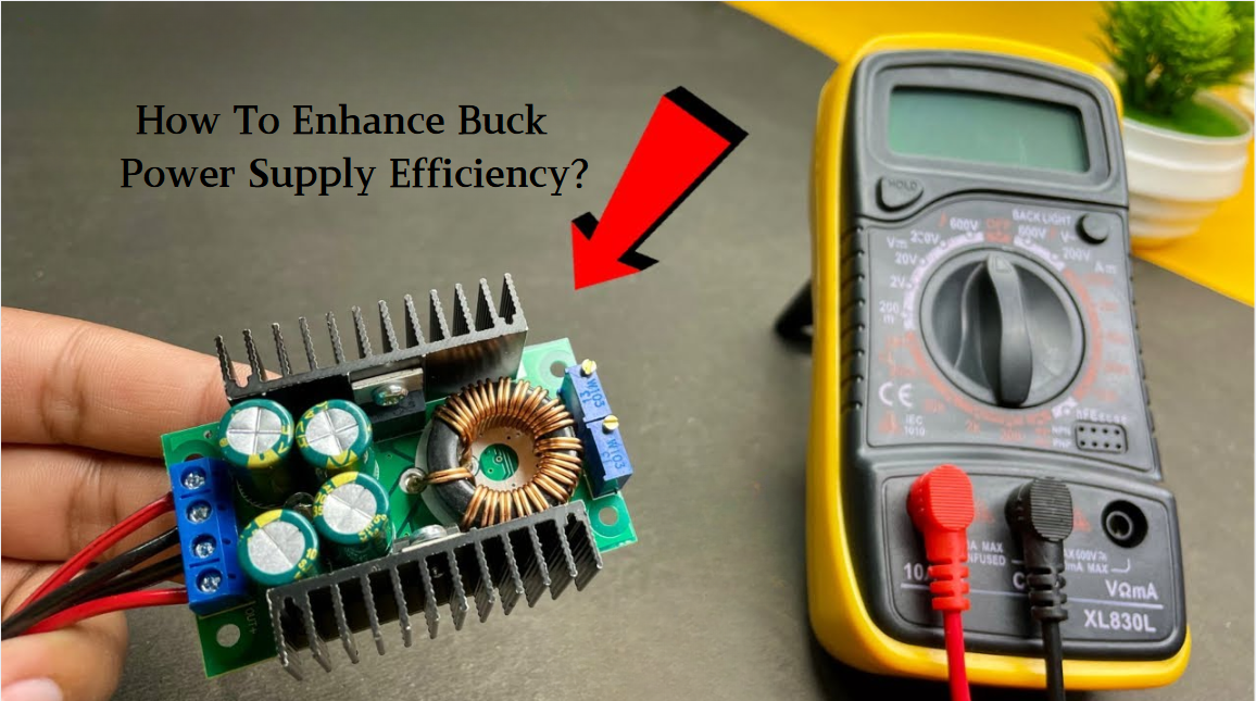
Key Strategies to Enhance Buck Power Supply Efficiency
Improving the efficiency of Buck (step-down) switching power supplies requires a multi-dimensional approach targeting energy loss sources, including component selection, topology optimization, control strategies, and thermal management. Below are core strategies and engineering practices:...
-
2025 / 06 / 26
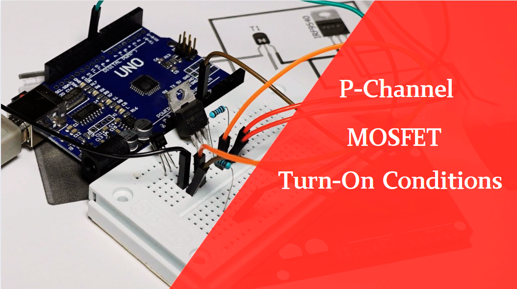
P-Channel MOSFET Turn-On Conditions
The turn-on conditions for a P-channel MOSFET (PMOS) are inverse to those of an N-channel MOSFET (NMOS), primarily governed by the relationship between the gate-source voltage (VGS) and the threshold voltage (Vth), along with voltage polarity. Here are the key points:A PMOS turns on when its gate vo...
-
2025 / 06 / 24
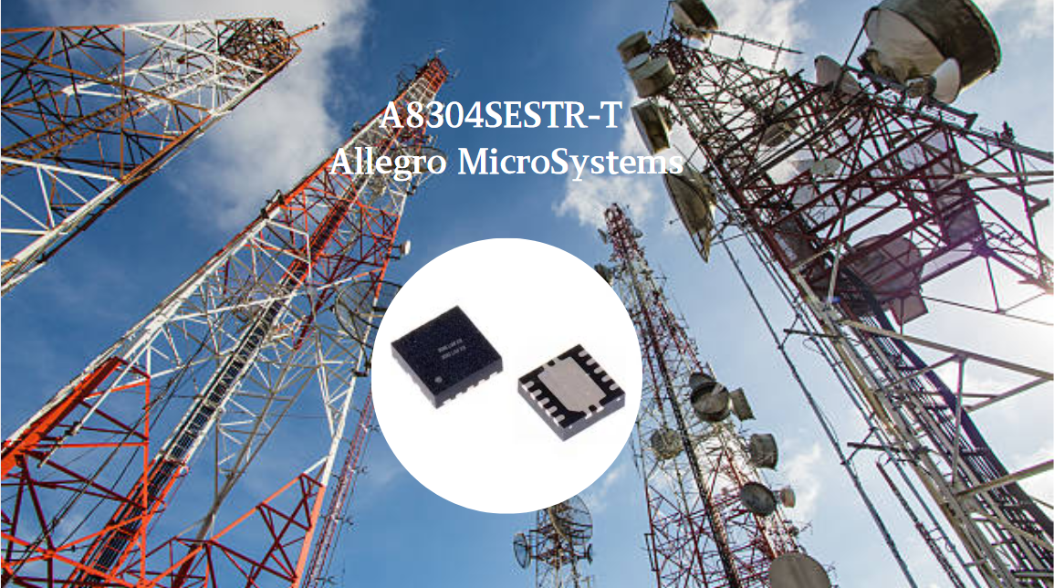
A8304SESTR-T Allegro MicroSystems-Single LNB Supply and Control Voltage Regulator
The Allegro MicroSystems A8304SESTR-T is a single-channel Low Noise Block Regulator (LNBR). It integrates a monolithic boost converter with MOSFET, current sensing, and compensation. Featuring a 704 kHz switching frequency, it uses few external components. With an I²C-compatible interface, it offers...
-
2025 / 06 / 20
EG25GGC-128-SGNS by Quectel Wireless Solutions Co., Ltd: Features,Symbol,Footprint and Datasheet
The Quectel EG25GGC - 128 - SGNS is an LTE Cat 4 module optimized for M2M and IoT. Supporting 3GPP Rel. 11, it offers up to 150Mbps downlink and 50Mbps uplink. With global LTE/UMTS/GSM coverage, it's backward - compatible with EDGE/GPRS. Featuring multi - constellation GNSS (GPS, GLONASS, BeiDou, et...

-
2025 / 06 / 17
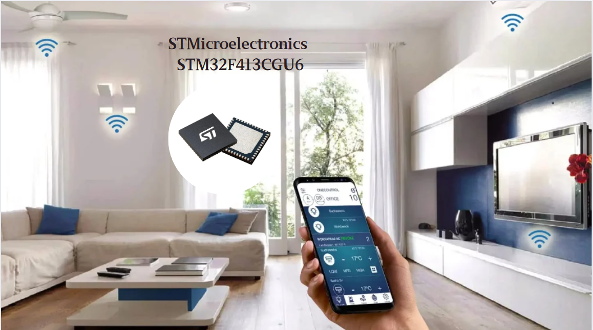
STMicroelectronics STM32F413CGU6 Microcontroller: Datasheet, Performance, Features
The STMicroelectronics STM32F413CGU6 is an Arm® Cortex®-M4 based MCU with FPU, operating at up to 100 MHz for 125 DMIPS performance. It features 1MB Flash, 320KB SRAM, and interfaces like USB OTG FS, 3 CAN, ADC, 2 DAC, and multiple serial ports. With low-power modes (Sleep, Stop, Standby), it suits ...
-
2025 / 06 / 13
STMicroelectronics STM32F446ZCT6 -Microcontrollers: A Comprehensive Guide
The STMicroelectronics STM32F446ZCT6 is an ARM Cortex-M4-based MCU with FPU, running at up to 180 MHz. It features 256 KB Flash, 128 KB SRAM + 4 KB backup SRAM, and offers rich peripherals: USB OTG HS/FS, 2 CAN, 3 ADCs, 17 timers, and 20 communication interfaces. In LQFP144 package, industrial temp ...

-
2025 / 06 / 09
MC33887PNB NXP Semiconductors-Motor Drivers:A Comprehensive Guide
The NXP Semiconductors MC33887PNB is a 5.0 A H - bridge power IC with integrated load current feedback. It operates across a 5.0 V - 28 V voltage range, features low RDS(on) (120 mΩ typical), and supports up to 10 kHz PWM. With functions like active current limiting and fault reporting, it ensures r...

-
2025 / 06 / 07
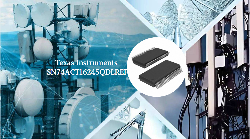
A 16-bit Bus Transceiver: Why Choose the Texas Instruments SN74ACT16245QDLREP?
The Texas Instruments SN74ACT16245QDLREP is a high-performance 16-bit bus transceiver. Designed for harsh industrial and automotive environments, it operates reliably from -40°C to +125°C. With its dual 8-bit non-inverting 3-state architecture, it enables efficient bidirectional data transfer. It of...

2000+
Daily average RFQ Volume

30,000,000
Standard Product Unit

2800+
Worldwide Manufacturers

15,000 m2
In-stock Warehouse
 Wishlist (0 Items)