

- RFQ
- BOM
-
Contact Us
Tel: +86-0755-83501315
Email: sales@sic-components.com


- Chinese
- English
- French
- German
- Portuguese
- Spanish
- Russian
- Japanese
- Korean
- Arabic
- Irish
- Greek
- Turkish
- Italian
- Danish
- Romanian
- Indonesian
- Czech
- Afrikaans
- Swedish
- Polish
- Basque
- Catalan
- Esperanto
- Hindi
- Lao
- Albanian
- Amharic
- Armenian
- Azerbaijani
- Belarusian
- Bengali
- Bosnian
- Bulgarian
- Cebuano
- Chichewa
- Corsican
- Croatian
- Dutch
- Estonian
- Filipino
- Finnish
- Frisian
- Galician
- Georgian
- Gujarati
- Haitian
- Hausa
- Hawaiian
- Hebrew
- Hmong
- Hungarian
- Icelandic
- Igbo
- Javanese
- Kannada
- Kazakh
- Khmer
- Kurdish
- Kyrgyz
- Latin
- Latvian
- Lithuanian
- Luxembou..
- Macedonian
- Malagasy
- Malay
- Malayalam
- Maltese
- Maori
- Marathi
- Mongolian
- Burmese
- Nepali
- Norwegian
- Pashto
- Persian
- Punjabi
- Serbian
- Sesotho
- Sinhala
- Slovak
- Slovenian
- Somali
- Samoan
- Scots Gaelic
- Shona
- Sindhi
- Sundanese
- Swahili
- Tajik
- Tamil
- Telugu
- Thai
- Ukrainian
- Urdu
- Uzbek
- Vietnamese
- Welsh
- Xhosa
- Yiddish
- Yoruba
- Zulu
- Kinyarwanda
- Tatar
- Oriya
- Turkmen
- Uyghur
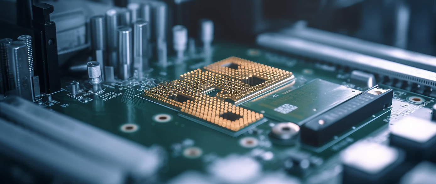
PCB Transistors: A Comprehensive Guide
This "Practical Guide to PCB Transistors" comprehensively and thoroughly introduces the relevant knowledge of PCB transistors, and it is of great reference value for both beginners in electronic design and experienced engineers.
I. Guide Overview
This guide is detailed, covering everything from the basic working principles of PCB transistors to advanced selection criteria and testing methods. We will delve deep into the basic transistor types and their characteristics, the key parameters for transistor selection, the practical testing techniques using common tools, the practical applications in modern electronic products, and the emerging trends in transistor technology. Whether you are designing a new circuit or diagnosing an existing one, this guide can provide you with the essential knowledge for effectively using PCB transistors.
II. Basic Knowledge of Transistors: Working Principles
Basic Working Principles: A transistor is a three-terminal semiconductor device that controls the current between the other two terminals (collector/drain and emitter/source) through the third control terminal (base/gate). This control mechanism has two main functions: first, amplification, that is, a small change in the controlled current or voltage can cause a large change in the output current; second, switching, which can be used as an electronically controlled on/off switch.
Semiconductor Physics behind Transistors: The operation of transistors is based on the characteristics of P-type and N-type semiconductor materials and their junctions. Doping refers to the intentional addition of impurities to silicon to generate charge carriers; the depletion region is the area where the mobile charges are depleted at the PN junction; the movement of charge carriers involves electrons and holes as current carriers. The interaction of these elements enables the transistor to control the current with high precision.
III. Main Types of PCB Transistors
Bipolar Junction Transistor (BJT): It is composed of three layers of alternating semiconductor materials (NPN or PNP) and has three terminals: emitter, base, and collector. It is a current-controlled device, where the base current can control the collector current. It has a medium input impedance and good linearity, making it suitable for amplification. Common packages include TO-92 (for small signals) and TO-220 (for power applications).
Field-Effect Transistor (FET): It has three terminals: source, gate, and drain. The channel between the source and the drain is controlled by the gate voltage. It has two subtypes: MOSFET (Metal-Oxide-Semiconductor Field-Effect Transistor) and JFET (Junction Field-Effect Transistor). MOSFET is further divided into enhancement mode (normally off) and depletion mode (normally on), while JFET has a relatively simple structure and is usually in the depletion mode. FET is a voltage-controlled device, with high input impedance, excellent switching performance, and low static power consumption. Different packages have different uses and thermal performances. TO-92 is used for low-power signals and has poor thermal performance; SOT-23 is an SMD small-signal package with medium thermal performance; TO-220 is used for power applications and has good thermal performance when equipped with a heat sink; D2PAK is a high-power SMD package with excellent thermal performance.
IV. Practical Testing Methods
Basic Continuity Testing: A digital multimeter (DMM) is required, and a component tester is optional. When testing a BJT, first identify the pinout (refer to the data sheet), test the base-emitter and base-collector junctions (which should behave like diodes), and verify that there is no conduction between the collector and the emitter when there is no base current. When testing an FET, check the gate-channel diode (MOSFET body diode), verify the change in the channel resistance with the gate bias, and test the gate leakage current.
Advanced Characteristic Testing: Curve tracing analysis can visually display the transistor characteristics, measure the breakdown voltage, and determine the gain curve. Online testing includes measuring the voltage at the operating point, signal tracing with an oscilloscope, and hot spot thermal imaging.
V. Common Applications of Transistors in PCBs
Analog Circuits: Transistors can be used in audio amplifiers (class A, B, AB), voltage regulators, oscillators, sensor interfaces, etc.
Digital Circuits: They are applied in logic gates, microcontroller I/Os, power switching, memory cells, etc.
Power Electronics: Suitable for DC-DC converters, motor drivers, power supplies, inverters, etc.
VI. Troubleshooting: Common Transistor Problems
Failure Modes: Including short circuits, such as collector-emitter/drain-source short circuits and gate oxide breakdown (for MOSFETs); open circuits, such as bonding wire failures and package cracking; performance degradation, such as reduced gain, increased leakage, and thermal runaway.
Diagnostic Techniques: Diagnosis can be carried out through visual inspection (checking for burn marks and package damage), resistance measurement, gain testing, thermal analysis, and other methods.
VII. Emerging Trends in Transistor Technology
Wide Bandgap Semiconductors: Silicon carbide (SiC) has a higher breakdown voltage and better thermal conductivity; gallium nitride (GaN) has faster switching speed and higher efficiency.
3D Transistor Structures: FinFET technology can improve gate control and reduce leakage; nanowire transistors represent the direction of next-generation miniaturization.
Integrated Smart Transistors: With built-in protection circuits, on-chip temperature sensing, and self-diagnosis functions.
VIII. Best Practices for PCB Design Using Transistors
Layout Considerations: Pay attention to thermal management (such as the design of copper pouring and vias), optimization of the gate/base drive circuit, minimizing parasitic effects, and adopting techniques to reduce EMI.
Reliability Enhancement: Follow the appropriate derating (80% rule), do a good job of ESD protection, eliminate mechanical stress, and use conformal coating in harsh environments.
IX. Conclusion: Mastering PCB Transistors
To have an in-depth understanding of PCB transistors, you need to master the relevant knowledge of semiconductor physics, electrical characteristics, practical testing methods, and specific applications. After mastering this knowledge, you will be able to select the most suitable transistor for different applications, design more reliable circuits with appropriate margins, effectively troubleshoot problems when they occur, and keep up with the development trend of transistor technology.
As electronic systems continue to evolve, transistor technology remains at the core of innovation. Whether using traditional silicon devices or cutting-edge wide bandgap semiconductors, the principles covered in this guide lay a solid foundation for using PCB transistors in various applications.
If you want to study further, it is recommended to explore manufacturer application notes, SPICE simulation models, conduct practical experiments using different transistor types, and study advanced semiconductor physics texts. By combining theoretical knowledge with practical experience, you can acquire the professional skills to effectively use transistors in all electronic designs.
https://www.sic-components.com/discrete-semiconductor-products/transistors

Hot Products
View More-

2P25U3H/38 Altech Corporation
-
IEGF66-33724-25-UV Sensata-Airpax
-
IULZXK1-1-52-70.0-GK-B3 Sensata-Airpax
-
SMCJ60CAHM3_A/I Vishay General Semiconductor - Diodes Division
-
TA45-ABFRT090C0-AZM12 SCHURTER Inc.
-
LA070URD31LI0350 Littelfuse Inc.
-
ROV10H781K-S Littelfuse Inc.
-

LFCL-UHA Littelfuse Inc.
-
TA45-ABFXKJ02C0 SCHURTER Inc.
-
LFR600602C Littelfuse Inc.
-
TA45-ABFGS060C0-AZM12 SCHURTER Inc.
-
0674001.DRT4 Littelfuse Inc.
Related Blogs
-
2025 / 06 / 30
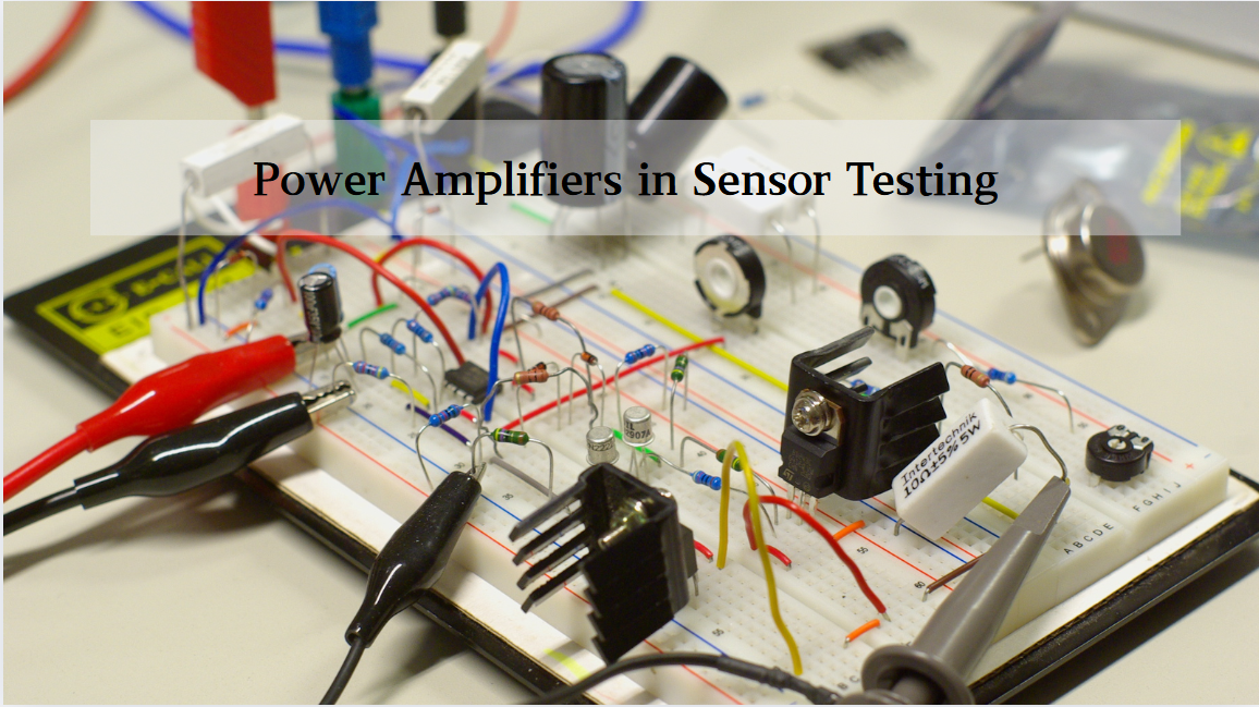
Multivariate Application Analysis of Power Amplifiers in Sensor Testing
In the field of modern sensor testing, power amplifiers (PAs) serve as core components and play an indispensable role. From amplifying weak signals to simulating complex physical environments, power amplifiers provide solid guarantees for the precise testing of sensor performance through their uniqu...
-
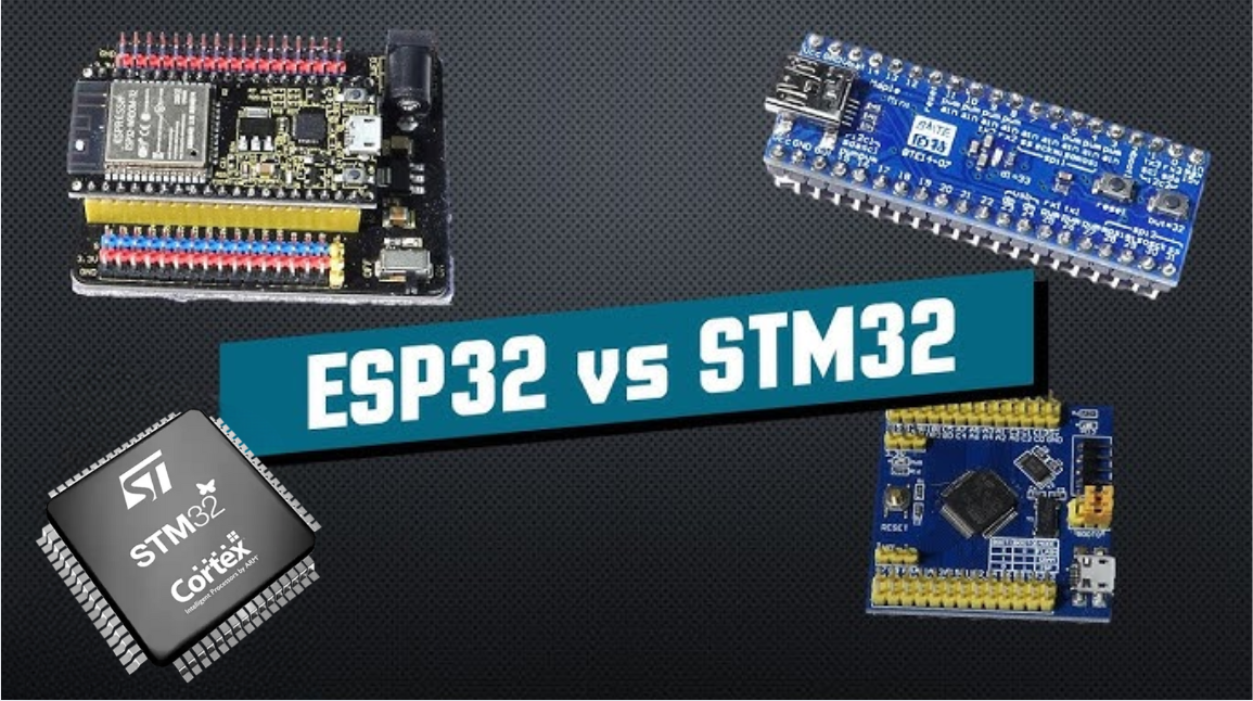
2025 / 06 / 28
ESP32 vs STM32: Which Microcontroller Suits You Better?
In the field of embedded development, both ESP32 and STM32 are highly favored microcontrollers, each with unique features and advantages. When facing project development, how do you choose between them? This requires comprehensive consideration of multiple factors. The following detailed comparison ...
-
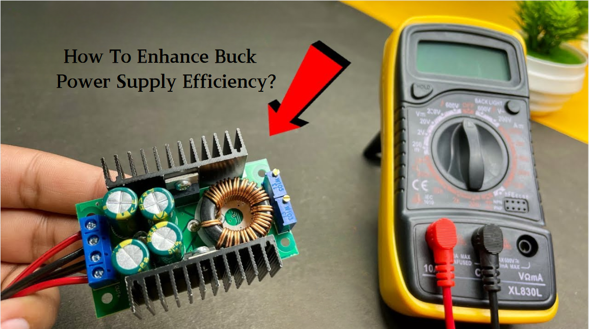
2025 / 06 / 26
Key Strategies to Enhance Buck Power Supply Efficiency
Improving the efficiency of Buck (step-down) switching power supplies requires a multi-dimensional approach targeting energy loss sources, including component selection, topology optimization, control strategies, and thermal management. Below are core strategies and engineering practices:...
-
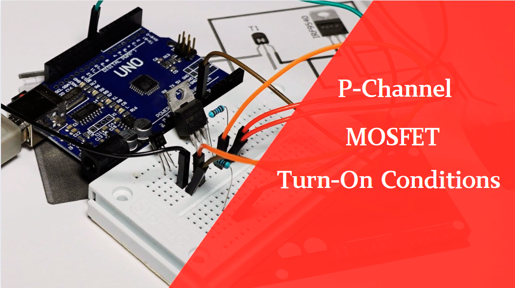
2025 / 06 / 26
P-Channel MOSFET Turn-On Conditions
The turn-on conditions for a P-channel MOSFET (PMOS) are inverse to those of an N-channel MOSFET (NMOS), primarily governed by the relationship between the gate-source voltage (VGS) and the threshold voltage (Vth), along with voltage polarity. Here are the key points:A PMOS turns on when its gate vo...
-
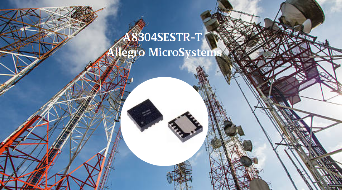
2025 / 06 / 24
A8304SESTR-T Allegro MicroSystems-Single LNB Supply and Control Voltage Regulator
The Allegro MicroSystems A8304SESTR-T is a single-channel Low Noise Block Regulator (LNBR). It integrates a monolithic boost converter with MOSFET, current sensing, and compensation. Featuring a 704 kHz switching frequency, it uses few external components. With an I²C-compatible interface, it offers...
-
2025 / 06 / 20
EG25GGC-128-SGNS by Quectel Wireless Solutions Co., Ltd: Features,Symbol,Footprint and Datasheet
The Quectel EG25GGC - 128 - SGNS is an LTE Cat 4 module optimized for M2M and IoT. Supporting 3GPP Rel. 11, it offers up to 150Mbps downlink and 50Mbps uplink. With global LTE/UMTS/GSM coverage, it's backward - compatible with EDGE/GPRS. Featuring multi - constellation GNSS (GPS, GLONASS, BeiDou, et...

-
2025 / 06 / 17
STMicroelectronics STM32F413CGU6 Microcontroller: Datasheet, Performance, Features
The STMicroelectronics STM32F413CGU6 is an Arm® Cortex®-M4 based MCU with FPU, operating at up to 100 MHz for 125 DMIPS performance. It features 1MB Flash, 320KB SRAM, and interfaces like USB OTG FS, 3 CAN, ADC, 2 DAC, and multiple serial ports. With low-power modes (Sleep, Stop, Standby), it suits ...

-
2025 / 06 / 13
STMicroelectronics STM32F446ZCT6 -Microcontrollers: A Comprehensive Guide
The STMicroelectronics STM32F446ZCT6 is an ARM Cortex-M4-based MCU with FPU, running at up to 180 MHz. It features 256 KB Flash, 128 KB SRAM + 4 KB backup SRAM, and offers rich peripherals: USB OTG HS/FS, 2 CAN, 3 ADCs, 17 timers, and 20 communication interfaces. In LQFP144 package, industrial temp ...

-
2025 / 06 / 09
MC33887PNB NXP Semiconductors-Motor Drivers:A Comprehensive Guide
The NXP Semiconductors MC33887PNB is a 5.0 A H - bridge power IC with integrated load current feedback. It operates across a 5.0 V - 28 V voltage range, features low RDS(on) (120 mΩ typical), and supports up to 10 kHz PWM. With functions like active current limiting and fault reporting, it ensures r...

-
2025 / 06 / 07
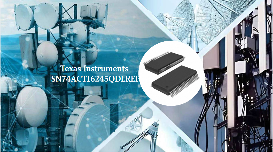
A 16-bit Bus Transceiver: Why Choose the Texas Instruments SN74ACT16245QDLREP?
The Texas Instruments SN74ACT16245QDLREP is a high-performance 16-bit bus transceiver. Designed for harsh industrial and automotive environments, it operates reliably from -40°C to +125°C. With its dual 8-bit non-inverting 3-state architecture, it enables efficient bidirectional data transfer. It of...

2000+
Daily average RFQ Volume

30,000,000
Standard Product Unit

2800+
Worldwide Manufacturers

15,000 m2
In-stock Warehouse
 Wishlist (0 Items)