

- RFQ
- BOM
-
Contact Us
Tel: +86-0755-83501315
Email: sales@sic-components.com


- Chinese
- English
- French
- German
- Portuguese
- Spanish
- Russian
- Japanese
- Korean
- Arabic
- Irish
- Greek
- Turkish
- Italian
- Danish
- Romanian
- Indonesian
- Czech
- Afrikaans
- Swedish
- Polish
- Basque
- Catalan
- Esperanto
- Hindi
- Lao
- Albanian
- Amharic
- Armenian
- Azerbaijani
- Belarusian
- Bengali
- Bosnian
- Bulgarian
- Cebuano
- Chichewa
- Corsican
- Croatian
- Dutch
- Estonian
- Filipino
- Finnish
- Frisian
- Galician
- Georgian
- Gujarati
- Haitian
- Hausa
- Hawaiian
- Hebrew
- Hmong
- Hungarian
- Icelandic
- Igbo
- Javanese
- Kannada
- Kazakh
- Khmer
- Kurdish
- Kyrgyz
- Latin
- Latvian
- Lithuanian
- Luxembou..
- Macedonian
- Malagasy
- Malay
- Malayalam
- Maltese
- Maori
- Marathi
- Mongolian
- Burmese
- Nepali
- Norwegian
- Pashto
- Persian
- Punjabi
- Serbian
- Sesotho
- Sinhala
- Slovak
- Slovenian
- Somali
- Samoan
- Scots Gaelic
- Shona
- Sindhi
- Sundanese
- Swahili
- Tajik
- Tamil
- Telugu
- Thai
- Ukrainian
- Urdu
- Uzbek
- Vietnamese
- Welsh
- Xhosa
- Yiddish
- Yoruba
- Zulu
- Kinyarwanda
- Tatar
- Oriya
- Turkmen
- Uyghur
Overview of IC Packaging: Types and Applications
In the ever - evolving landscape of electronics, integrated circuit (IC) packaging (https://www.sic-components.com/category-all) is a critical aspect that often remains hidden from the end - user's view but is essential for the functionality, reliability, and performance of electronic devices. From the smallest wearable gadgets to the most powerful supercomputers, IC packaging plays a pivotal role in bringing semiconductor components to life and integrating them into larger systems.
The Building Blocks of IC Packages
Die
At the very heart of an IC package lies the die, a tiny slice of silicon that contains the intricate circuitry responsible for the device's specific functions. The die is where all the electronic operations, such as data processing, signal amplification, and logic operations, take place. It is fabricated using a complex series of processes including photolithography, doping, and etching to create transistors, capacitors, and other components at the microscopic level.
Leadframe
The leadframe is typically made of thin metal, commonly copper or an alloy steel. It serves a dual - purpose function. Electrically, it provides the external connection points, or pins, through which the IC communicates with other components on the printed circuit board (PCB). Mechanically, it offers a sturdy foundation for the die, supporting it during the manufacturing process and throughout the device's lifetime. The design of the leadframe, including the number, shape, and spacing of the pins, is carefully engineered to meet the electrical and mechanical requirements of the IC.
Substrate
The substrate acts as the base for mounting the die and other components. It facilitates both electrical connections between the die and the external pins and provides additional mechanical support to the entire package. Substrates can be constructed from various materials. Laminates like FR - 4 and BT are cost - effective options commonly used in mass - produced consumer electronics. Ceramics, such as alumina and aluminum nitride, offer high thermal conductivity, making them suitable for applications where efficient heat dissipation is crucial, like in high - power electronics. There are also flexible substrates, such as those used in tape - automated bonding (TAB), which provide flexibility in design and assembly.
Wire Bonds
Wire bonds are microscopic wires, usually made of gold or aluminum, that create the electrical link between the die and the leadframe or substrate. These tiny wires act as conduits, transmitting electrical signals between the internal circuitry of the die and the external pins of the package. The quality and reliability of wire bonds are critical, as any breakage or degradation can lead to a failure in the IC's operation. Advanced bonding techniques, such as ball bonding and wedge bonding, are used to ensure strong and reliable connections.
Encapsulant
The encapsulant, typically an epoxy resin - based molding compound, encloses and safeguards the entire assembly, including the die, leadframe, wires, and substrate. It offers several important benefits. Mechanically, it provides structural integrity to the package, protecting the delicate internal components from physical damage. Environmentally, it shields the components from contaminants like dust, moisture, and corrosive gases. Some encapsulants also play a role in thermal management, helping to dissipate heat generated by the die.
The Developments of IC Packaging Process
The journey of IC packaging development has been driven by the relentless pursuit of miniaturization, enhanced performance, and increased functionality. In the early days, through - hole packages like the Dual In - line Package (DIP) were the norm. These packages were relatively large and had a limited pin count, but they were easy to handle and assemble, making them suitable for the electronics of that era.
The 1970s marked a significant milestone with the introduction of the Ball Grid Array (BGA) packages. BGA packages replaced the traditional lead - based connections with an array of solder balls on the underside of the package. This innovation allowed for a much higher pin count and a smaller footprint, enabling the development of more complex and powerful ICs.
As the 21st century dawned, new packaging technologies emerged to meet the growing demands of the electronics industry. Plastic Quad Flat Pack (PQFP) and Thin Small Outline Package (TSOP) became popular, offering better space utilization and improved performance compared to previous designs. The Land Grid Array (LGA) packages, especially those promoted by companies like Intel, further reduced the package size and improved electrical performance.
The development continued with the advent of Flip - Chip Ball Grid Arrays (FCBGAs). Unlike traditional BGAs, FCBGAs distribute input and output signals across the entire die surface, rather than just the edges. This design enhancement significantly improved the electrical performance and functionality of modern electronic devices, enabling high - speed data transfer and processing.
Types of IC Packaging
Integrated Circuit (IC) packaging is a crucial aspect of electronics manufacturing, safeguarding semiconductor components and enabling their integration into various devices. There is a diverse range of IC packaging types, each designed to meet specific performance, size, and cost requirements. Here are some of the most common types:
1. Dual In - line Package (DIP)
Structure: DIP is one of the oldest and most recognizable IC package types. It features a rectangular body with two parallel rows of pins extending perpendicularly from the sides. The pins are spaced at a standard 2.54 mm (0.1 inches), which makes it compatible with through - hole printed circuit board (PCB) technology. For example, an 8 - pin DIP has four pins on each side, and larger DIPs can have up to 64 pins or more.
Advantages:
Simplicity and Ease of Use: DIPs are straightforward to handle and insert into PCBs, making them ideal for hobbyists, prototyping, and educational projects. They can be easily soldered by hand, and the use of IC sockets allows for quick component replacement.
Cost - effective: The manufacturing process for DIPs is relatively simple, resulting in lower production costs, especially for low - volume applications.
Mechanical Stability: The through - hole mounting provides good mechanical support, making the package suitable for applications where the PCB may be subject to some physical stress or vibration.
Disadvantages:
Large Footprint: Compared to modern surface - mount packages, DIPs occupy a significant amount of space on the PCB, limiting the density of components that can be integrated.
Limited Pin Count: As the demand for more complex circuits grew, the pin count limitations of DIPs became a constraint. Their design is not well - suited for high - pin - count applications.
Electrical Performance: The long leads of DIPs introduce higher inductance and capacitance, which can degrade the electrical performance, especially at high frequencies.
Applications: DIPs are still used in some legacy systems, simple consumer electronics like basic calculators, and in educational kits due to their ease of use and low cost.
2. Small Outline Package (SOP)
Structure: SOPs are surface - mount packages that are smaller and more compact than DIPs. They have a rectangular shape with leads that extend outward from two sides of the package body in a gull - wing or J - lead configuration. The lead pitch (distance between adjacent leads) is typically smaller than that of DIPs, often around 1.27 mm or less, allowing for a more dense component layout on the PCB.
Advantages:
Space Efficiency: SOPs offer a significant reduction in footprint compared to DIPs, enabling more components to be placed on a PCB. This is crucial for miniaturized electronic devices.
Surface - mount Compatibility: They are designed for surface - mount technology (SMT), which is more automated and efficient than through - hole assembly, leading to higher production volumes and lower assembly costs for mass - produced products.
Disadvantages:
Manual Soldering Difficulty: While SMT is more automated, manual soldering of SOPs can be more challenging than DIPs due to the smaller lead size and closer spacing. Specialized soldering tools and skills are required.
Limited Pin Count for Some Variants: Although SOPs can have more pins than DIPs in some cases, for very high - pin - count applications, other package types may be more suitable.
Applications: SOPs are widely used in a variety of consumer electronics, such as mobile phones, digital cameras, and portable music players, as well as in many low - to - medium - complexity integrated circuits like operational amplifiers and small - scale microcontrollers.
3. Quad Flat Package (QFP)
Structure: QFP packages have a square or rectangular body with leads extending from all four sides. This design allows for a much higher pin count compared to DIPs and SOPs. Pin counts can range from 32 to over 256, with lead pitches typically in the range of 0.4 - 1.0 mm. There are also variations such as the Low - profile Quad Flat Package (LQFP) and Thin Quad Flat Package (TQFP), which are thinner versions of the standard QFP, further reducing the package height.
Advantages:
High Pin Count: QFPs are capable of accommodating a large number of pins, making them suitable for complex integrated circuits like microcontrollers, digital signal processors (DSPs), and some application - specific integrated circuits (ASICs).
Good Thermal and Electrical Performance: The multiple - sided lead arrangement and larger surface area of the package can contribute to better heat dissipation and electrical signal integrity compared to some other packages with fewer connection points.
Disadvantages:
Assembly Complexity: The small lead pitch and large number of pins make QFP assembly more challenging. Specialized SMT equipment and precise soldering techniques are required to ensure proper soldering and avoid short circuits between adjacent pins.
Higher Cost: Due to the more complex manufacturing process and the need for advanced assembly methods, QFP packages are generally more expensive than simpler package types like DIPs.
Applications: QFPs are commonly used in high - performance electronics, including automotive electronics for engine control units, industrial control systems, and many types of embedded computing devices.
4. Ball Grid Array (BGA)
Structure: BGA packages represent a significant departure from traditional lead - based packages. Instead of leads, they have an array of small solder balls on the underside of the package. These solder balls are used to establish electrical connections between the IC and the PCB. The balls are arranged in a grid pattern, and the package can have a very high pin count, often exceeding 1000 pins in some advanced versions. The ball pitch (distance between adjacent balls) typically ranges from 0.5 - 1.27 mm.
Advantages:
High Pin Density: BGA packages offer the highest pin count in a relatively small footprint, enabling the integration of highly complex circuits. This is essential for high - end processors, graphics processing units (GPUs), and advanced networking chips.
Improved Electrical Performance: The short interconnects between the solder balls and the PCB result in lower inductance and capacitance, which improves signal integrity and allows for high - speed data transfer. Additionally, the distributed nature of the connections helps in better power and ground distribution.
Good Thermal Management: The large surface area of the BGA package and the direct contact of the solder balls with the PCB provide an efficient path for heat dissipation, making it suitable for high - power - consuming devices.
Disadvantages:
Assembly and Rework Complexity: BGA assembly requires specialized equipment, such as pick - and - place machines and reflow ovens, and strict process control to ensure proper soldering of the solder balls. Reworking a faulty BGA component is extremely challenging and often requires advanced techniques and equipment.
Inspection Difficulty: Since the solder balls are on the underside of the package, visual inspection for soldering defects is not possible without the use of X - ray inspection equipment.
Applications: BGA packages are widely used in high - performance computing, gaming consoles, server motherboards, and high - end networking equipment where high pin counts, excellent electrical performance, and efficient thermal management are critical.
5. Chip Scale Package (CSP)
Structure: CSPs are designed to be as small as possible, with the package size typically being only slightly larger than the size of the die itself, usually within 1.2 times the die size. They can use various connection methods, such as solder balls similar to BGA or fine - pitch leads. CSPs often have a very thin profile, with a package height of 1 mm or less, and a fine pitch between contacts, typically in the range of 0.4 - 0.8 mm.
Advantages:
Miniaturization: CSPs enable the development of extremely small and compact electronic devices. Their small size is ideal for applications where space is at a premium, such as in wearable devices, smartphones, and other portable electronics.
Improved Electrical Performance: The short interconnects in CSPs reduce signal delays and package parasitics, resulting in better electrical performance, especially for high - speed signals.
Cost - effective in High - Volume: Although the initial development and manufacturing costs of CSPs can be high, in high - volume production, the reduced use of materials and the potential for simpler assembly processes can lead to cost savings.
Disadvantages:
Assembly and Rework Challenges: Similar to BGA, the small size and fine - pitch nature of CSPs make assembly and rework difficult. Specialized equipment and skilled operators are required to handle and solder these packages accurately.
Thermal Management: Due to the small size and close proximity of the die to the package surface, efficient heat dissipation can be a challenge, especially for high - power - consuming chips.
Applications: CSPs are commonly found in mobile devices, IoT sensors, high - density memory modules, and other miniaturized electronic products where size and performance are key considerations.
6. System - in - Package (SiP)
Structure: SiP is not just a physical package type but an integration concept. It involves integrating multiple discrete components, such as different types of ICs (e.g., microcontrollers, memory chips, RF modules), passive components (resistors, capacitors), and sometimes even sensors or antennas, all within a single package. The components can be stacked vertically, placed side - by - side, or a combination of both, and are interconnected using various techniques like wire bonding, flip - chip bonding, or embedded traces within the package substrate.
Advantages:
High Integration Density: SiP allows for the creation of highly integrated systems in a single package, reducing the overall size and weight of the final product compared to using separate PCBs for each component. This is beneficial for portable and space - constrained applications.
Improved Performance: By integrating components in close proximity, signal delays and interference can be minimized, leading to improved system performance. Additionally, power consumption can be optimized through better power management within the package.
Design Flexibility: SiP offers designers the flexibility to combine different components from various suppliers, tailoring the package to specific application requirements without having to develop a custom - integrated circuit.
Disadvantages:
Complex Design and Assembly: Designing and assembling SiP modules require advanced design tools and techniques, as well as expertise in handling multiple component types and integration methods. This can increase the design and development costs.
Testing Complexity: Testing a SiP is more complex than testing individual components, as faults can be difficult to isolate within the integrated package. Specialized test equipment and procedures are needed.
Applications: SiP is widely used in smartphones, where it can integrate the application processor, memory, and wireless communication modules. It is also used in other portable devices, IoT devices, and some aerospace and military electronics for its ability to create compact, high - performance systems.
7. Multi - Chip Module (MCM)
Structure: MCMs involve mounting multiple semiconductor chips or dies onto a common substrate, which can be made of materials like ceramic or organic laminates. The chips are interconnected using various methods, such as wire bonding, flip - chip bonding, or a combination of both. The substrate provides electrical connections between the chips, as well as a mechanical support structure. MCMs can integrate different types of chips, including microprocessors, memory chips, and ASICs, to create a complete functional subsystem.
Advantages:
High - level Integration: MCMs enable the integration of multiple chips into a single module, reducing the overall size and complexity of the electronic system compared to using separate PCBs for each chip. This can lead to improved performance, reduced power consumption, and better reliability.
Customization: Designers can select and combine different chips based on the specific requirements of the application, allowing for a high degree of customization. This is useful in applications where off - the - shelf solutions may not meet all the needs.
Improved Signal Integrity: By reducing the length of interconnects between chips, MCMs can improve signal integrity, especially for high - speed signals.
Disadvantages:
High Cost: The development and manufacturing of MCMs are expensive due to the use of high - quality substrates, advanced interconnection techniques, and the need for precise assembly and testing processes.
Yield and Reliability Challenges: Integrating multiple chips in a single module increases the complexity of the manufacturing process, which can lead to lower yields and potential reliability issues. If one chip in the MCM fails, the entire module may need to be replaced.
Applications: MCMs are used in high - performance computing systems, telecommunications equipment, and some military and aerospace applications where high - level integration, customization, and reliable performance are essential.
Materials and Selection Considerations https://www.sic-components.com/category-all
Leadframe Materials
Copper and its alloys are popular choices for leadframes due to their good electrical conductivity and mechanical strength. Iron - nickel alloys are also used in some applications where specific magnetic or thermal properties are required. The selection of leadframe material depends on factors such as the electrical requirements of the IC, the mechanical stress it will endure, and the cost - performance balance.
Substrate Materials
Laminates: FR - 4 and BT laminates are cost - effective and widely used in mass - produced consumer electronics. They offer good mechanical strength and electrical insulation properties.
Ceramics: Alumina and aluminum nitride ceramics are preferred for high - performance applications due to their high thermal conductivity, excellent electrical insulation, and mechanical stability. They can withstand high temperatures and harsh environments.
Flexible Substrates: Materials like polyimide are used in flexible substrates for applications where flexibility and bendability are required, such as in wearable devices and some automotive electronics.
Wire Bond Materials
Gold: Gold wire bonds offer superior conductivity, excellent corrosion resistance, and high - reliability. However, they are relatively expensive, which limits their use in cost - sensitive applications.
Copper: Copper wire bonds provide a good compromise between performance and cost. They have high conductivity and are becoming increasingly popular as bonding techniques improve to address issues such as oxidation.
Aluminum: Aluminum wire bonds are the most cost - effective option. They are commonly used in applications where cost is a major factor, but they may have lower reliability compared to gold and copper in some environments.
Encapsulant Materials
Epoxy Molding Compounds: These are the most commonly used encapsulants due to their affordability, ease of use, and good mechanical and electrical properties. However, they are hygroscopic, which can lead to issues in high - humidity environments.
Ceramics: Ceramic encapsulants offer hermetic sealing, excellent thermal performance, and high - reliability. They are used in applications where long - term reliability and resistance to harsh environments are critical, such as in aerospace and military electronics.
Resins: Specialized resins are used in some applications to meet specific requirements, such as high - temperature resistance or chemical resistance.
Factors Influencing Package Selection
Performance Requirements
Electrical Performance: The package must meet the desired electrical performance, including signal integrity, power integrity, and thermal management. For high - speed applications, packages with low inductance and capacitance are required to minimize signal distortion and delay.
Thermal Performance: Efficient heat dissipation is crucial for the reliable operation of ICs, especially in high - power applications. Packages with good thermal conductivity, such as those with exposed pads, heat spreaders, or heat sinks, are preferred to prevent overheating.
High - Frequency Performance: In applications operating at high frequencies, such as RF and microwave, the package must have low parasitics and minimal signal loss. Specialized packages, such as cavity packages or air - cavity packages, may be required to achieve the desired high - frequency performance.
Cost
The cost of the IC package is an important consideration, especially for mass - produced consumer electronics. Factors such as the package material, manufacturing process, and volume pricing can significantly impact the overall cost. Engineers need to balance the cost of the package against the required performance and reliability to ensure the cost - effectiveness of the final product.
Manufacturing Constraints
Compatibility with Manufacturing Processes: The package must be compatible with the available PCB assembly processes and equipment. Considerations such as package size, lead pitch, and assembly requirements should be taken into account to ensure manufacturability. For example, some advanced packages may require specialized SMT assembly equipment and processes, which can increase the manufacturing complexity and cost.
Yield and Quality Control: The manufacturing process of the IC package should be able to achieve high yields and ensure consistent quality. Advanced packages with tight tolerances and complex manufacturing steps may have lower yields, which can impact the production cost and delivery schedule.
Size and Space Constraints
The size and footprint of the IC package are important factors, especially in applications where space is limited, such as in portable devices and wearable electronics. Smaller packages allow for higher component density on PCBs, enabling the development of more compact and lightweight products. However, smaller packages may also have limitations in terms of thermal performance and pin count.
Reliability
The IC package must provide adequate protection against environmental factors, such as moisture, shock, and vibration, to ensure reliable operation over the product's lifetime. Packages with hermetic sealing, robust mechanical construction, and good thermal management are more likely to meet the reliability requirements of demanding applications.
Why is IC Packaging Important?
Protection
IC packaging provides essential protection to the delicate semiconductor die. It shields the die from physical damage, such as mechanical shock and vibration, which can occur during handling, transportation, and operation of the electronic device. The encapsulant also protects the die from environmental contaminants, such as dust, moisture, and corrosive gases, which can cause corrosion and degradation of the internal circuitry over time.
Electrical Connection
The package provides the electrical connections between the IC and other components on the PCB. The leadframe or solder balls in the package act as the interface through which electrical signals are transmitted to and from the IC. Proper electrical connection is crucial for the correct operation of the IC and the overall electronic system.
Thermal Management
ICs generate heat during operation, and effective thermal management is essential to prevent overheating, which can lead to performance degradation and even failure of the IC. The package plays a vital role in thermal management by facilitating the transfer of heat from the die to the PCB and ultimately to the surrounding environment. Packages with good thermal conductivity, heat spreaders, and heat sinks help to dissipate heat more efficiently, ensuring the IC operates within its optimal temperature range.
Integration
IC packaging enables the integration of the IC into the larger electronic system. It provides a standardized form factor and interface that allows the IC to be easily mounted and connected to the PCB. This integration is essential for the functionality and performance of modern electronic devices, which often consist of multiple ICs and other components working together.
Challenges and Limitations
Package - Induced Stress
Differences in the thermal expansion coefficients between the package materials and the silicon die can lead to mechanical stress on the die. This stress can cause die cracking, delamination, or performance degradation over time. To address this challenge, manufacturers use low - stress packaging materials with similar thermal expansion coefficients to the die and implement stress - relief features, such as underfill materials or compliant interconnects.
Thermal Dissipation Limits
As ICs become more powerful and operate at higher frequencies, the amount of heat generated increases. However, there are limits to how much heat can be dissipated through the package. This can lead to overheating, reduced performance, and reliability issues. Advanced thermal management techniques, such as the use of high - thermal - conductivity materials, enhanced heat spreaders, and more efficient heat sinks, are being developed to overcome these limitations.
Signal Integrity Issues
High - speed and high - frequency signals are more susceptible to crosstalk, reflections, and electromagnetic interference (EMI) due to the package parasitics and interconnect characteristics. These signal integrity issues can degrade the performance of the IC and the overall electronic system. To mitigate these problems, engineers use controlled impedance design techniques, ground planes, shielding, and advanced packaging technologies that minimize package parasitics.
Manufacturing Complexity
Advanced IC packages, such as BGAs, CSPs, and 3D packages, require precise manufacturing processes and tight tolerances. The complexity of these manufacturing processes can lead to increased costs, lower yields, and potential reliability issues. Manufacturers need to invest in advanced manufacturing equipment, skilled labor, and quality control measures to ensure the successful production of these advanced packages.
Electrical Performance Limitations
IC packages introduce electrical limitations, such as increased resistance, inductance, and capacitance, which can impact the device's performance, power efficiency, and signal integrity. These limitations become more significant as the operating frequencies of ICs increase. To improve electrical performance, manufacturers use low - resistance materials for package interconnects, optimize package layout, and employ advanced packaging technologies that reduce interconnect lengths.
Cost Considerations
Advanced IC packaging technologies, such as flip - chip BGAs and wafer - level packages, can be more expensive than traditional packaging methods due to their increased complexity and specialized manufacturing processes. This higher cost can be a barrier to their widespread adoption, especially in cost - sensitive applications. Engineers need to carefully evaluate the cost - benefit ratio of different packaging options to ensure the most cost - effective solution for their specific applications.
In conclusion, IC packaging is a complex and crucial field that encompasses a wide range of technologies, materials, and considerations. As the electronics industry continues to evolve, the development of IC packaging will play an increasingly important role in enabling the creation of smaller, faster, more powerful, and more reliable electronic devices.
https://www.sic-components.com/category-all


Hot Products
View More-
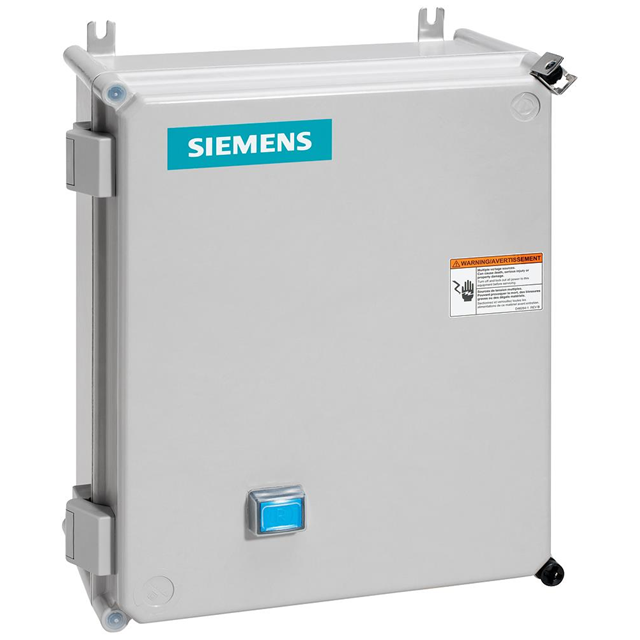
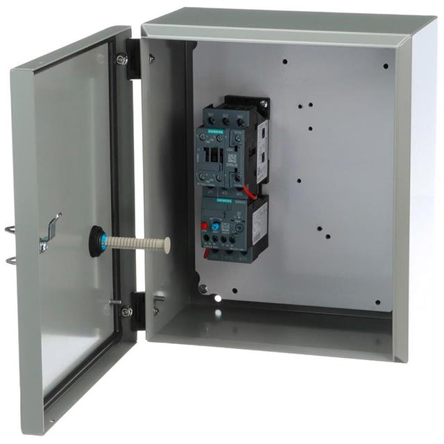
US2:14CUA32FG Siemens
-

R88A-CN111A Omron Automation and Safety
-
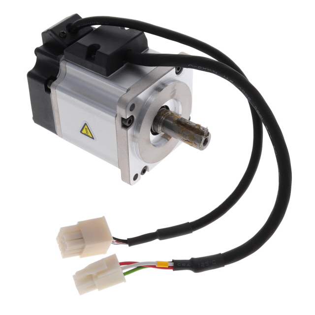
MSMF092L1B1 Panasonic Industrial Automation Sales
-
DRA3R40B2 Sensata-Crydom
-
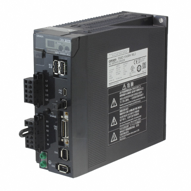
R88D-GT04L Omron Automation and Safety
-
3RA21101EA151BB4 Siemens
-
MSMF041L1T2 Panasonic Industrial Automation Sales
-
R88A-CNEA01C-E Omron Automation and Safety
-
R88A-CA1C01SFR-A Omron Automation and Safety
-
17CUC92NA10 Siemens
-
US2:14CUC12AC Siemens
-
MHME502SCC Panasonic Industrial Automation Sales
Related Blogs
-
2025 / 06 / 30
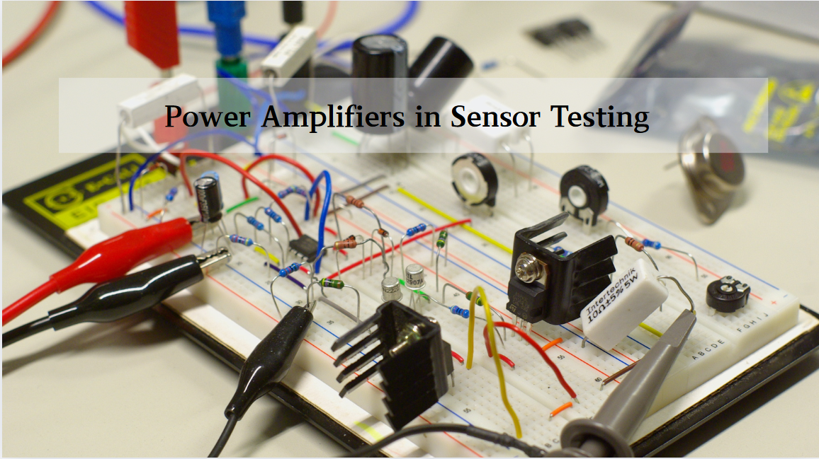
Multivariate Application Analysis of Power Amplifiers in Sensor Testing
In the field of modern sensor testing, power amplifiers (PAs) serve as core components and play an indispensable role. From amplifying weak signals to simulating complex physical environments, power amplifiers provide solid guarantees for the precise testing of sensor performance through their uniqu...
-
2025 / 06 / 28
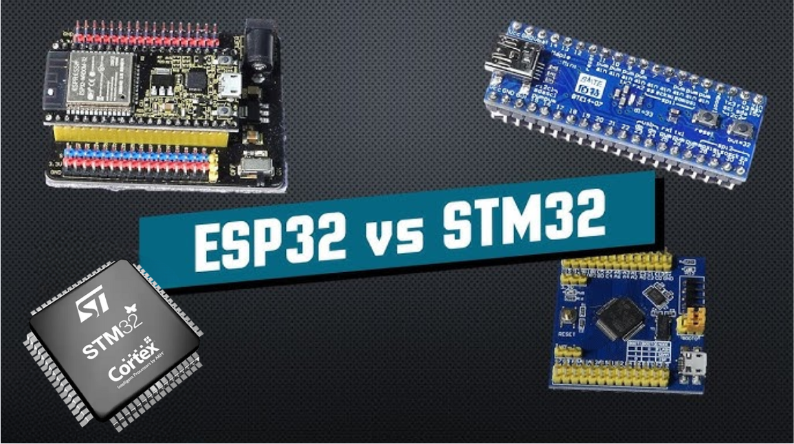
ESP32 vs STM32: Which Microcontroller Suits You Better?
In the field of embedded development, both ESP32 and STM32 are highly favored microcontrollers, each with unique features and advantages. When facing project development, how do you choose between them? This requires comprehensive consideration of multiple factors. The following detailed comparison ...
-
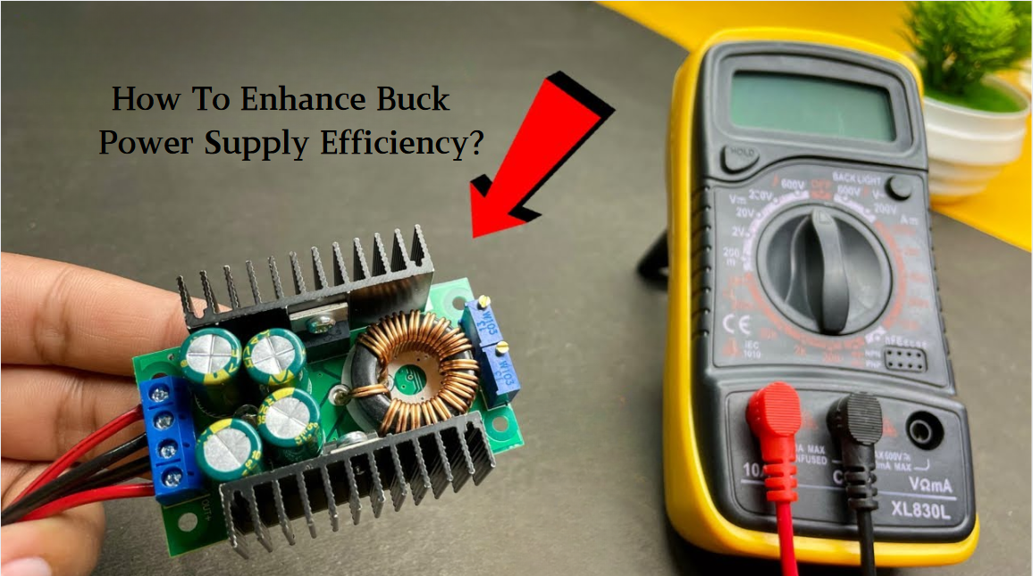
2025 / 06 / 26
Key Strategies to Enhance Buck Power Supply Efficiency
Improving the efficiency of Buck (step-down) switching power supplies requires a multi-dimensional approach targeting energy loss sources, including component selection, topology optimization, control strategies, and thermal management. Below are core strategies and engineering practices:...
-
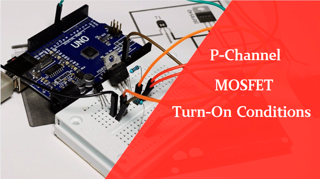
2025 / 06 / 26
P-Channel MOSFET Turn-On Conditions
The turn-on conditions for a P-channel MOSFET (PMOS) are inverse to those of an N-channel MOSFET (NMOS), primarily governed by the relationship between the gate-source voltage (VGS) and the threshold voltage (Vth), along with voltage polarity. Here are the key points:A PMOS turns on when its gate vo...
-
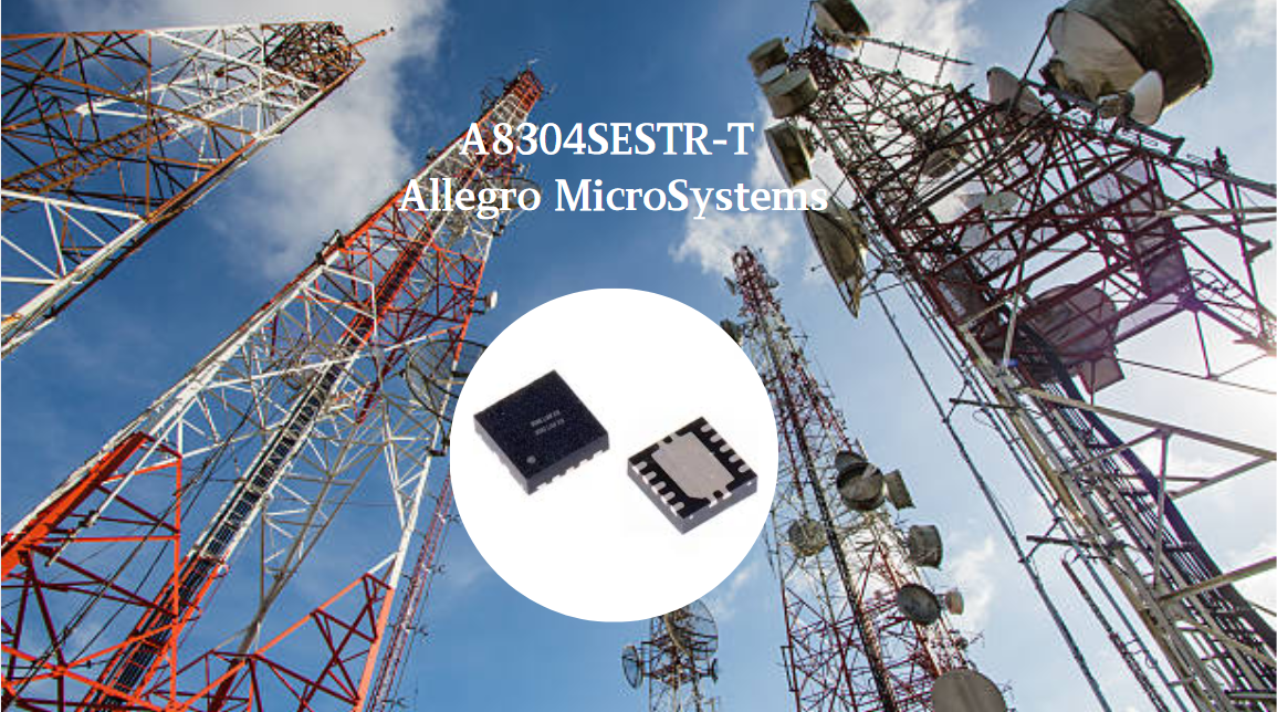
2025 / 06 / 24
A8304SESTR-T Allegro MicroSystems-Single LNB Supply and Control Voltage Regulator
The Allegro MicroSystems A8304SESTR-T is a single-channel Low Noise Block Regulator (LNBR). It integrates a monolithic boost converter with MOSFET, current sensing, and compensation. Featuring a 704 kHz switching frequency, it uses few external components. With an I²C-compatible interface, it offers...
-
2025 / 06 / 20
EG25GGC-128-SGNS by Quectel Wireless Solutions Co., Ltd: Features,Symbol,Footprint and Datasheet
The Quectel EG25GGC - 128 - SGNS is an LTE Cat 4 module optimized for M2M and IoT. Supporting 3GPP Rel. 11, it offers up to 150Mbps downlink and 50Mbps uplink. With global LTE/UMTS/GSM coverage, it's backward - compatible with EDGE/GPRS. Featuring multi - constellation GNSS (GPS, GLONASS, BeiDou, et...

-
2025 / 06 / 17
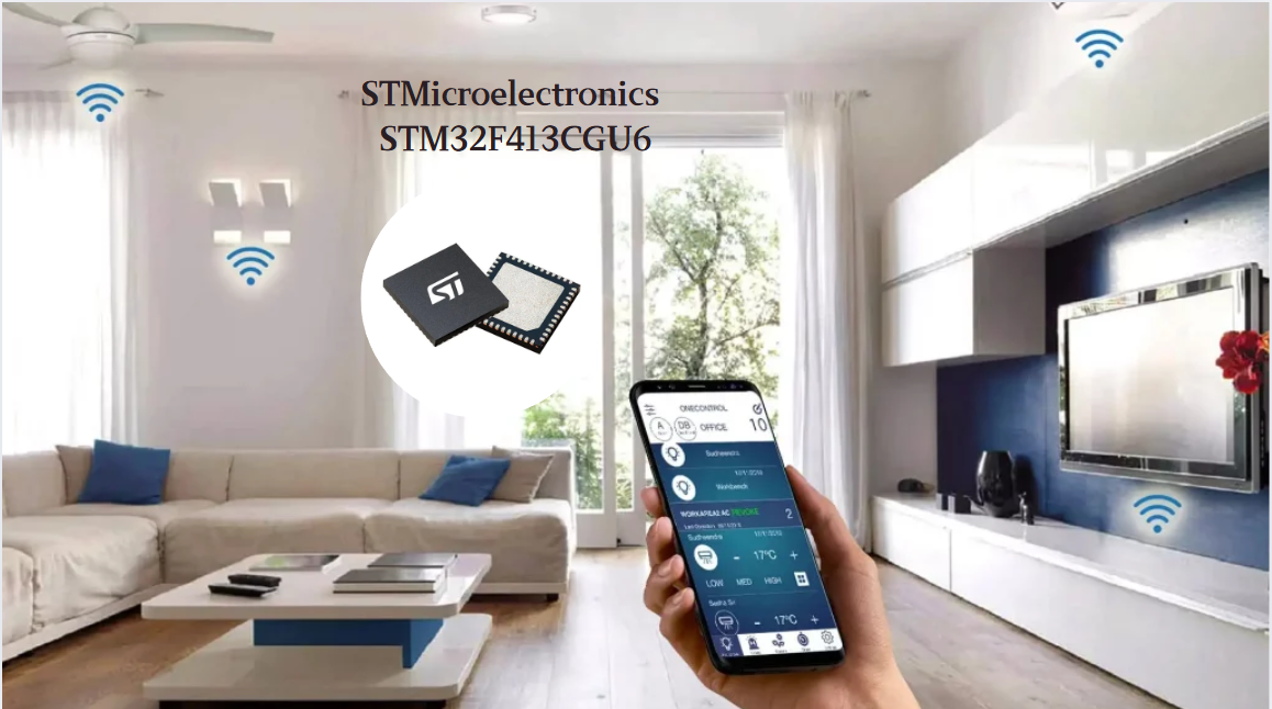
STMicroelectronics STM32F413CGU6 Microcontroller: Datasheet, Performance, Features
The STMicroelectronics STM32F413CGU6 is an Arm® Cortex®-M4 based MCU with FPU, operating at up to 100 MHz for 125 DMIPS performance. It features 1MB Flash, 320KB SRAM, and interfaces like USB OTG FS, 3 CAN, ADC, 2 DAC, and multiple serial ports. With low-power modes (Sleep, Stop, Standby), it suits ...
-
2025 / 06 / 13
STMicroelectronics STM32F446ZCT6 -Microcontrollers: A Comprehensive Guide
The STMicroelectronics STM32F446ZCT6 is an ARM Cortex-M4-based MCU with FPU, running at up to 180 MHz. It features 256 KB Flash, 128 KB SRAM + 4 KB backup SRAM, and offers rich peripherals: USB OTG HS/FS, 2 CAN, 3 ADCs, 17 timers, and 20 communication interfaces. In LQFP144 package, industrial temp ...

-
2025 / 06 / 09
MC33887PNB NXP Semiconductors-Motor Drivers:A Comprehensive Guide
The NXP Semiconductors MC33887PNB is a 5.0 A H - bridge power IC with integrated load current feedback. It operates across a 5.0 V - 28 V voltage range, features low RDS(on) (120 mΩ typical), and supports up to 10 kHz PWM. With functions like active current limiting and fault reporting, it ensures r...

-
2025 / 06 / 07
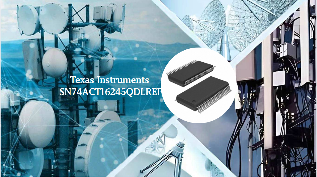
A 16-bit Bus Transceiver: Why Choose the Texas Instruments SN74ACT16245QDLREP?
The Texas Instruments SN74ACT16245QDLREP is a high-performance 16-bit bus transceiver. Designed for harsh industrial and automotive environments, it operates reliably from -40°C to +125°C. With its dual 8-bit non-inverting 3-state architecture, it enables efficient bidirectional data transfer. It of...

2000+
Daily average RFQ Volume

30,000,000
Standard Product Unit

2800+
Worldwide Manufacturers

15,000 m2
In-stock Warehouse
 Wishlist (0 Items)