

- RFQ
- BOM
-
Contact Us
Tel: +86-0755-83501315
Email: sales@sic-components.com


- Chinese
- English
- French
- German
- Portuguese
- Spanish
- Russian
- Japanese
- Korean
- Arabic
- Irish
- Greek
- Turkish
- Italian
- Danish
- Romanian
- Indonesian
- Czech
- Afrikaans
- Swedish
- Polish
- Basque
- Catalan
- Esperanto
- Hindi
- Lao
- Albanian
- Amharic
- Armenian
- Azerbaijani
- Belarusian
- Bengali
- Bosnian
- Bulgarian
- Cebuano
- Chichewa
- Corsican
- Croatian
- Dutch
- Estonian
- Filipino
- Finnish
- Frisian
- Galician
- Georgian
- Gujarati
- Haitian
- Hausa
- Hawaiian
- Hebrew
- Hmong
- Hungarian
- Icelandic
- Igbo
- Javanese
- Kannada
- Kazakh
- Khmer
- Kurdish
- Kyrgyz
- Latin
- Latvian
- Lithuanian
- Luxembou..
- Macedonian
- Malagasy
- Malay
- Malayalam
- Maltese
- Maori
- Marathi
- Mongolian
- Burmese
- Nepali
- Norwegian
- Pashto
- Persian
- Punjabi
- Serbian
- Sesotho
- Sinhala
- Slovak
- Slovenian
- Somali
- Samoan
- Scots Gaelic
- Shona
- Sindhi
- Sundanese
- Swahili
- Tajik
- Tamil
- Telugu
- Thai
- Ukrainian
- Urdu
- Uzbek
- Vietnamese
- Welsh
- Xhosa
- Yiddish
- Yoruba
- Zulu
- Kinyarwanda
- Tatar
- Oriya
- Turkmen
- Uyghur
Low Offset Voltage Amplifier
I. Basic Concepts and Technical Definitions
A Low Offset Voltage Amplifier is a type of analog integrated circuit characterized by extremely low input offset voltage (Vos), which reduces the output deviation to the microvolt (μV) level when the input is zero through circuit design and process optimization. In an ideal operational amplifier (op-amp), zero input should yield zero output, but in reality, transistor mismatch and process variations require a tiny input voltage (Vos) to null the output. Typical low-offset products can achieve Vos below 1μV (e.g., ADI's AD8610 with Vos = 0.5μV), far lower than general-purpose op-amps (10–100μV). (https://www.sic-components.com/integrated-circuits-ics/linear/amplifierscategory-1/special-purpose-amplifiers?page=12)
II. Key Technical Specifications and Performance Parameters
Parameter Definition Typical Range Impact Scenarios
Offset Voltage (Vos) The input voltage difference required to make the output zero 0.5μV–50μV Precision in amplifying weak signals
Offset Voltage Drift (TC Vos) The change in Vos per 1°C temperature variation 0.01μV/°C–5μV/°C Long-term stability in wide temperature ranges
Open-Loop Gain (Aol) Voltage amplification without feedback >110dB Closed-loop gain accuracy and linearity
Common-Mode Rejection Ratio (CMRR) Ability to suppress common-mode signals, reflecting noise resistance >100dB Anti-interference for sensor differential signals
Input Bias Current (Ibias) Bias current required at the input terminals 1pA–1nA Matching high-impedance signal sources (e.g., piezoelectric sensors)
Noise Density (en) Noise voltage amplitude per unit bandwidth 1nV/√Hz–10nV/√Hz Signal-to-noise ratio for weak signals (e.g., bioelectrical detection)
III. Circuit Architectures and Implementation Technologies
1. Classic Architectural Designs
Three-Op-Amp Instrumentation Amplifier Structure: The front-end two op-amps buffer differential inputs, and the rear-end amplifies the difference. Symmetric design reduces offset (e.g., INA128 with Vos = 25μV).
Chopper Stabilization: High-frequency switching and filtering modulate low-frequency offset to high frequencies for elimination (e.g., LTC2057 with Vos < 1μV), but may introduce chopper spike noise.
Auto-Zero Technology: Real-time offset compensation using storage capacitors (e.g., OPA333 with Vos = 15μV), but suffers from "popcorn noise" and bandwidth limitations.
2. Process and Layout Optimization
Laser Trimming Technology: Post-fabrication laser trimming of resistor networks compensates for input-stage mismatch (e.g., AD707 op-amp with Vos calibrated to <10μV).
Common-Centroid Layout: Geometrically symmetric arrangement of differential pair transistors to reduce process gradient mismatch, suitable for CMOS and BJT processes.
SOI (Silicon-on-Insulator) Process: Reduces parasitic effects and improves device matching (e.g., TI's OPA2333 with Vos = 50μV).
IV. Typical Application Scenarios and Cases
1. Precision Sensor Signal Conditioning
Strain Gauges and Bridge Sensors: In electronic scales, a 100Ω strain gauge outputs ~100μV under 1kg pressure, requiring a low-offset op-amp (e.g., INA118, Vos = 50μV) to amplify signals to the ADC range (e.g., 0–5V) with gain error <0.01%.
Thermocouple Temperature Sensing: A Type K thermocouple generates ~40μV/°C at 0°C. Paired with a low-offset op-amp (e.g., AD8551, Vos = 25μV), it achieves 0.1°C temperature resolution.
2. Medical and Bioelectrical Signal Acquisition
ECG Front-End Amplification: Cardiac signals range from 0.1–5mV, requiring suppression of 100V-level power frequency common-mode interference. A typical solution uses INA333 (Vos = 15μV, CMRR = 120dB) with a right-leg drive circuit for noise reduction.
Neural Signal Recording: Neuronal discharge signals are as low as 10–100μV, requiring op-amps like OPA129 (Vos = 10μV, en = 1.1nV/√Hz) to ensure signals are not overwhelmed by offset and noise.
3. High-Precision Measuring Instruments
Digital Multimeters (DMMs): The 10nV range of Fluke 8846A relies on low-offset op-amps (e.g., AD797, Vos = 25μV) with 24-bit ADCs to achieve 1pA current detection.
Battery Management Systems (BMS): In lithium battery charge/discharge current detection, a 1mΩ shunt resistor generates 10mV under 10A current, requiring an op-amp (e.g., INA240, Vos = 50μV) for amplification with power calculation error <0.1%.
V. Selection Principles and Design Challenges
1. Parameter Matching Principles
Signal Amplitude vs. Vos: For a 100μV input signal, Vos should be <10μV (10% of the signal amplitude) to avoid significant errors.
Temperature Range vs. TC Vos: In industrial-grade (-40°C to +85°C) scenarios, a TC Vos of 1μV/°C introduces 125μV offset over 85°C, necessitating devices with TC Vos <0.1μV/°C (e.g., AD8606, TC Vos = 0.03μV/°C).
Power Consumption vs. Speed Balance: Low-power devices (e.g., LMP7721, 15μA quiescent current) suit battery-powered applications but may have limited bandwidth (100kHz), while high-speed scenarios require OPA690 (700V/μs slew rate, higher power consumption).
2. Circuit Design Pitfalls
PCB Layout Impact: Input-stage traces must be short and symmetric to avoid noise coupling; power terminals need 10μF + 0.1μF decoupling capacitors to suppress ripple (50mV power fluctuations may introduce 1μV offset with insufficient PSRR).
Capacitive Load Stability: For loads >100nF, an external RC compensation network (e.g., 100Ω in series with 1nF) is needed to prevent self-oscillation (e.g., OPA2277 driving 220nF without compensation may have phase margin <45°).
VI. Cutting-Edge Technologies and Future Trends
Digital-Assisted Calibration Technology
On-chip ADC and DSP monitor offset in real time, enabling dynamic compensation via digital algorithms (e.g., TI's DRV5032 integrates a 16-bit ADC, calibrating Vos to <1μV) for industrial automation real-time requirements.
Ultra-Low Power Integration with IoT
Sub-threshold design (e.g., Ambiq's APM32 op-amp, 1μA quiescent current, Vos = 20μV) adapts to wearable devices, supporting microwatt-level power operation for biosensors (e.g., heart rate monitoring).
Quantum and Extreme Environment Applications
Radiation-hardened devices (e.g., AD8609) for space detectors maintain Vos drift <5μV under 100kRad radiation; JFET input op-amps (e.g., OPA637, Vos = 100μV) preserve device characteristics in cryogenic environments (e.g., liquid helium at -269°C).
Heterogeneous Integration and Multifunctionality
Integration of low-offset op-amps with MEMS sensors (e.g., Bosch BMP388, with built-in 24-bit ADC and op-amp, Vos = 50μV) enables full signal chain calibration for pressure detection with error <0.1%.
VII. Industry Standards and Mainstream Manufacturer Product Matrices
Manufacturer Typical Product Vos Application Fields
Analog Devices (ADI) AD8610 0.5μV Quantum computing, medical imaging
Texas Instruments (TI) OPA188 2μV Industrial measurement, sensor interfaces
Linear Technology LTC6078 1μV Battery-powered devices, precision DAQ
Maxim Integrated MAX4197 5μV Automotive electronics, portable instruments
Microchip MCP6V01 10μV Consumer electronics, low-power sensors
As the "precision cornerstone" of analog circuits, low offset voltage amplifiers continue to evolve around the principles of "smaller error, lower power, and stronger adaptability". From traditional industrial detection to cutting-edge quantum computing, these devices drive continuous innovation in precision measurement and signal processing with μV-level control. In the future, with the integration of semiconductor processes and intelligent calibration technologies, low-offset op-amps will play a more critical role in IoT and extreme environment applications.
(https://www.sic-components.com/integrated-circuits-ics/linear/amplifierscategory-1/special-purpose-amplifiers?page=12)


Hot Products
View MoreRelated Blogs
-
2025 / 06 / 30
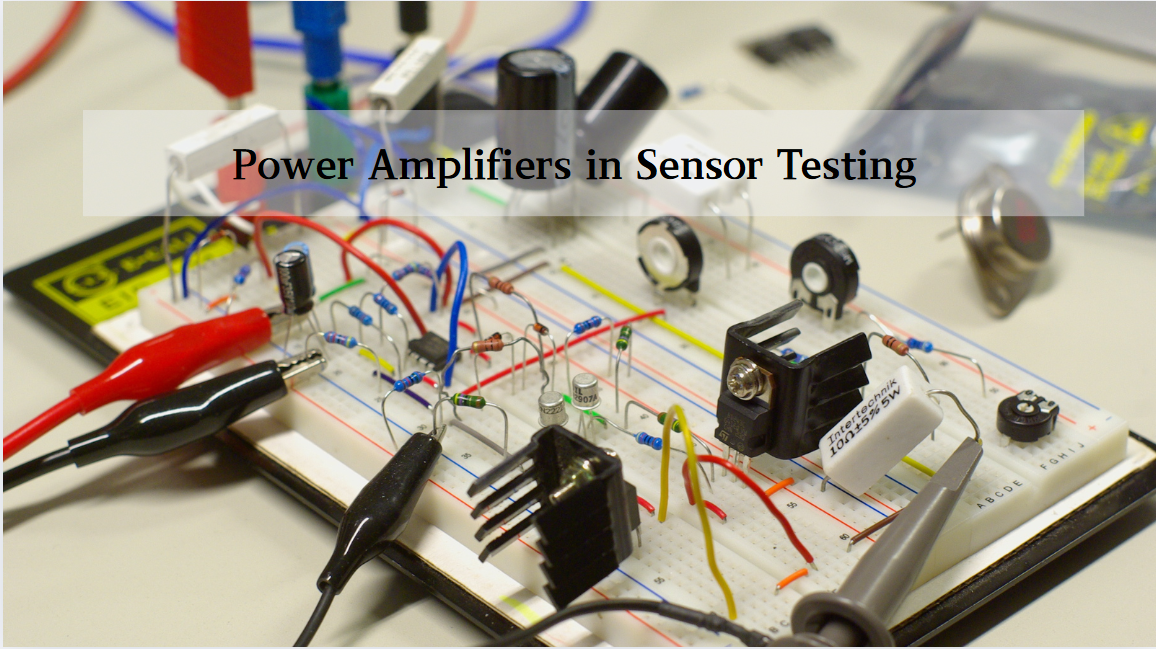
Multivariate Application Analysis of Power Amplifiers in Sensor Testing
In the field of modern sensor testing, power amplifiers (PAs) serve as core components and play an indispensable role. From amplifying weak signals to simulating complex physical environments, power amplifiers provide solid guarantees for the precise testing of sensor performance through their uniqu...
-
2025 / 06 / 28
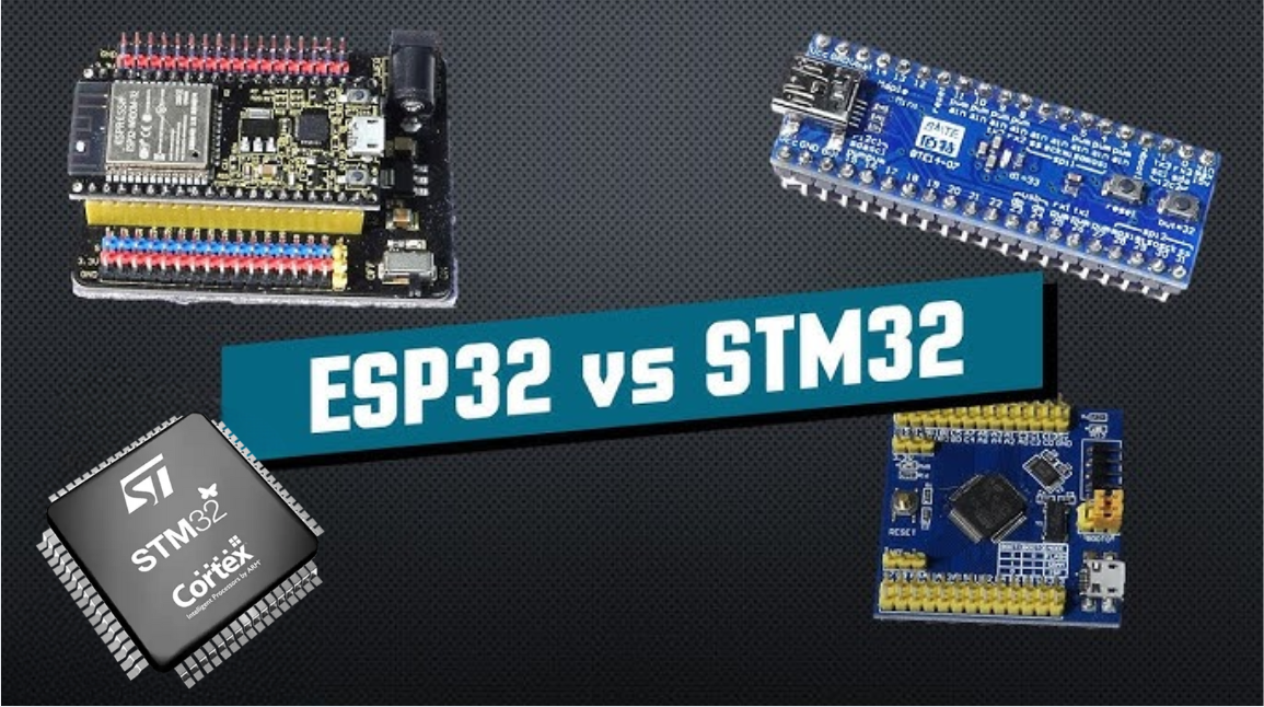
ESP32 vs STM32: Which Microcontroller Suits You Better?
In the field of embedded development, both ESP32 and STM32 are highly favored microcontrollers, each with unique features and advantages. When facing project development, how do you choose between them? This requires comprehensive consideration of multiple factors. The following detailed comparison ...
-
2025 / 06 / 26
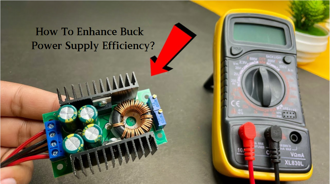
Key Strategies to Enhance Buck Power Supply Efficiency
Improving the efficiency of Buck (step-down) switching power supplies requires a multi-dimensional approach targeting energy loss sources, including component selection, topology optimization, control strategies, and thermal management. Below are core strategies and engineering practices:...
-
2025 / 06 / 26
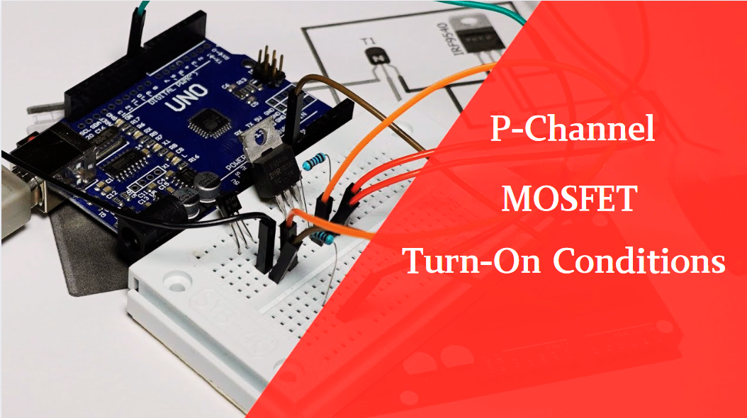
P-Channel MOSFET Turn-On Conditions
The turn-on conditions for a P-channel MOSFET (PMOS) are inverse to those of an N-channel MOSFET (NMOS), primarily governed by the relationship between the gate-source voltage (VGS) and the threshold voltage (Vth), along with voltage polarity. Here are the key points:A PMOS turns on when its gate vo...
-
2025 / 06 / 24
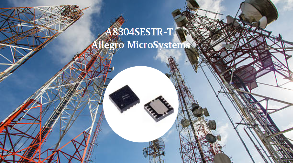
A8304SESTR-T Allegro MicroSystems-Single LNB Supply and Control Voltage Regulator
The Allegro MicroSystems A8304SESTR-T is a single-channel Low Noise Block Regulator (LNBR). It integrates a monolithic boost converter with MOSFET, current sensing, and compensation. Featuring a 704 kHz switching frequency, it uses few external components. With an I²C-compatible interface, it offers...
-
2025 / 06 / 20
EG25GGC-128-SGNS by Quectel Wireless Solutions Co., Ltd: Features,Symbol,Footprint and Datasheet
The Quectel EG25GGC - 128 - SGNS is an LTE Cat 4 module optimized for M2M and IoT. Supporting 3GPP Rel. 11, it offers up to 150Mbps downlink and 50Mbps uplink. With global LTE/UMTS/GSM coverage, it's backward - compatible with EDGE/GPRS. Featuring multi - constellation GNSS (GPS, GLONASS, BeiDou, et...

-
2025 / 06 / 17
STMicroelectronics STM32F413CGU6 Microcontroller: Datasheet, Performance, Features
The STMicroelectronics STM32F413CGU6 is an Arm® Cortex®-M4 based MCU with FPU, operating at up to 100 MHz for 125 DMIPS performance. It features 1MB Flash, 320KB SRAM, and interfaces like USB OTG FS, 3 CAN, ADC, 2 DAC, and multiple serial ports. With low-power modes (Sleep, Stop, Standby), it suits ...

-
2025 / 06 / 13
STMicroelectronics STM32F446ZCT6 -Microcontrollers: A Comprehensive Guide
The STMicroelectronics STM32F446ZCT6 is an ARM Cortex-M4-based MCU with FPU, running at up to 180 MHz. It features 256 KB Flash, 128 KB SRAM + 4 KB backup SRAM, and offers rich peripherals: USB OTG HS/FS, 2 CAN, 3 ADCs, 17 timers, and 20 communication interfaces. In LQFP144 package, industrial temp ...

-
2025 / 06 / 09
MC33887PNB NXP Semiconductors-Motor Drivers:A Comprehensive Guide
The NXP Semiconductors MC33887PNB is a 5.0 A H - bridge power IC with integrated load current feedback. It operates across a 5.0 V - 28 V voltage range, features low RDS(on) (120 mΩ typical), and supports up to 10 kHz PWM. With functions like active current limiting and fault reporting, it ensures r...

-
2025 / 06 / 07
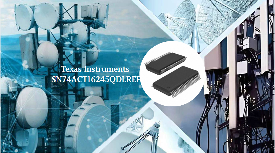
A 16-bit Bus Transceiver: Why Choose the Texas Instruments SN74ACT16245QDLREP?
The Texas Instruments SN74ACT16245QDLREP is a high-performance 16-bit bus transceiver. Designed for harsh industrial and automotive environments, it operates reliably from -40°C to +125°C. With its dual 8-bit non-inverting 3-state architecture, it enables efficient bidirectional data transfer. It of...

2000+
Daily average RFQ Volume

30,000,000
Standard Product Unit

2800+
Worldwide Manufacturers

15,000 m2
In-stock Warehouse
 Wishlist (0 Items)