- RFQ
- BOM
-
Contact Us
Tel: +86-0755-83501315
Email: sales@sic-components.com


- Chinese
- English
- French
- German
- Portuguese
- Spanish
- Russian
- Japanese
- Korean
- Arabic
- Irish
- Greek
- Turkish
- Italian
- Danish
- Romanian
- Indonesian
- Czech
- Afrikaans
- Swedish
- Polish
- Basque
- Catalan
- Esperanto
- Hindi
- Lao
- Albanian
- Amharic
- Armenian
- Azerbaijani
- Belarusian
- Bengali
- Bosnian
- Bulgarian
- Cebuano
- Chichewa
- Corsican
- Croatian
- Dutch
- Estonian
- Filipino
- Finnish
- Frisian
- Galician
- Georgian
- Gujarati
- Haitian
- Hausa
- Hawaiian
- Hebrew
- Hmong
- Hungarian
- Icelandic
- Igbo
- Javanese
- Kannada
- Kazakh
- Khmer
- Kurdish
- Kyrgyz
- Latin
- Latvian
- Lithuanian
- Luxembou..
- Macedonian
- Malagasy
- Malay
- Malayalam
- Maltese
- Maori
- Marathi
- Mongolian
- Burmese
- Nepali
- Norwegian
- Pashto
- Persian
- Punjabi
- Serbian
- Sesotho
- Sinhala
- Slovak
- Slovenian
- Somali
- Samoan
- Scots Gaelic
- Shona
- Sindhi
- Sundanese
- Swahili
- Tajik
- Tamil
- Telugu
- Thai
- Ukrainian
- Urdu
- Uzbek
- Vietnamese
- Welsh
- Xhosa
- Yiddish
- Yoruba
- Zulu
- Kinyarwanda
- Tatar
- Oriya
- Turkmen
- Uyghur
Flip Flop ICs
This article aims to provide a comprehensive exploration of Flip Flop ICs. We will begin by delving into the fundamental concepts that underpin their operation, including the principles of two - state systems and the role of feedback. A detailed comparison with latches will clarify their unique characteristics. Next, we will examine the four main types of Flip Flop ICs—SR, JK, D, and T—unpacking their structures, operations, truth tables, and characteristics equations. The working mechanisms, particularly the role of clock signals and state transitions, will be analyzed in depth. Following that, we will explore the diverse applications of Flip Flop ICs in digital memory, counters, shift registers, and sequential logic circuits.
1. Introduction
Definition and Significance
Flip Flop ICs, or integrated circuits, are semiconductor - based components that serve as the building blocks of flip flop circuits. At their essence, these circuits are binary - state systems, capable of existing in one of two stable conditions, typically denoted as logic 0 (low) and logic 1 (high). Flip Flop ICs act as the gatekeepers of these states, precisely controlling when and how transitions between them occur based on input signals.
In the realm of digital electronics, their significance cannot be overstated. Flip Flop ICs are the fundamental units responsible for data storage and transfer. In computers, they form the basis of registers, which hold data temporarily during processing, and are integral to memory cells that store information over longer periods. In communication systems, they enable the synchronization of data transmission, ensuring that bits are accurately received and interpreted. Whether it's in consumer electronics, industrial automation, or cutting - edge research equipment, any digital system that requires the manipulation and retention of binary data relies on Flip Flop ICs.
2. Fundamental Concepts of Flip Flop ICs
Basic Principles
At the heart of Flip Flop ICs lies the concept of two stable states. These states are like two distinct rooms, and the flip flop can "reside" in either one. The ability to maintain these states is what allows flip flops to store binary data. For instance, a logic 0 state might represent an "off" condition, while a logic 1 state represents an "on" condition.
Feedback plays a crucial role in the operation of flip flop circuits. Consider a simple analogy: imagine a room where the light switch's state is influenced not only by the direct action of flipping the switch but also by the current state of the light itself. In a flip flop circuit, the output of a gate is fed back to be processed alongside the input signal. This feedback loop creates a dependency on the previous state of the circuit, enabling the flip flop to "remember" and make decisions based on past conditions. For example, in some flip flop types, the output at a given moment can affect how the circuit responds to the next input, effectively creating a sequential behavior.
Differences from Latches
While Flip Flop ICs and latches share the ability to store data, the primary distinction lies in their triggering mechanisms. Latches are level - triggered devices. This means that when the enable input (or the level - sensitive control signal) is active, the latch continuously updates its output based on the input signals. In contrast, Flip Flop ICs are edge - triggered, relying on a clock signal. The clock signal acts as a conductor, dictating precisely when the flip flop should change its state.
To illustrate, consider an SR latch and an SR flip flop. In an SR latch, when the enable signal is high, a change in the S or R input immediately affects the output. However, in an SR flip flop, even if the S or R inputs change, the output will only be updated when the clock signal experiences a rising or falling edge. Simple circuit diagrams can further clarify this difference. In a latch circuit, the input directly influences the output when enabled, whereas in a flip flop circuit, the clock signal gates the input - output relationship, ensuring more controlled and synchronized operation.
3. Types of Flip Flop ICs
SR Flip - Flop
Structure and Inputs
The SR flip - flop, short for Set - Reset flip - flop, has two primary inputs: the Set (S) input and the Reset (R) input, along with a clock input (in clocked versions). The basic circuit structure often consists of cross - coupled NOR gates or NAND gates. When the Set input is activated (usually by a high signal in active - high configurations), it sets the output Q to 1 and the complementary output Q' to 0. Conversely, when the Reset input is triggered, Q is set to 0 and Q' to 1.
Operation
In normal operation, when both S and R are low (inactive), the flip - flop maintains its current state, thanks to the feedback mechanism. When S = 1 and R = 0, the flip - flop is set, and the output Q becomes 1. When S = 0 and R = 1, it is reset, and Q becomes 0. However, when both S and R are high simultaneously, the output enters an undefined state. This situation is avoided in practical designs as it can lead to unpredictable behavior.
Truth Table and Characteristics Equation
The truth table for an SR flip - flop presents all possible combinations of S, R, and the current state Q, along with the resulting next state Q(n + 1). For example:
S R Q Q(n + 1)
0 0 0 0
0 0 1 1
0 1 0 0
0 1 1 0
1 0 0 1
1 0 1 1
1 1 0 Undefined
1 1 1 Undefined
The characteristics equation, Q(n + 1)= S + R'Q, is derived from the truth table. It provides a mathematical representation to predict the next state of the flip - flop based on the current state and the input values.
JK Flip - Flop
Enhancements over SR Flip - Flop
The JK flip - flop addresses the major limitation of the SR flip - flop, which is the undefined state when both inputs are high. It offers more flexibility and reliable operation in all input combinations.
Inputs and Operation
The JK flip - flop has two inputs, J and K, in addition to the clock input. When J = 0 and K = 0, the flip - flop maintains its current state. When J = 0 and K = 1, it resets the output (Q = 0). When J = 1 and K = 0, it sets the output (Q = 1). The most interesting case is when J = K = 1. In this situation, at each clock edge, the output toggles, changing from 0 to 1 or vice versa. This toggle functionality makes the JK flip - flop useful in various applications, such as counters.
Truth Table and Characteristics Equation
The truth table for a JK flip - flop shows the relationship between J, K, the current state Q, and the next state Q(n + 1):
J K Q Q(n + 1)
0 0 0 0
0 0 1 1
0 1 0 0
0 1 1 0
1 0 0 1
1 0 1 1
1 1 0 1
1 1 1 0
The characteristics equation, Q(n + 1)= JQ' + K'Q, precisely describes how the next state of the flip - flop is determined based on the current state and the J and K inputs.
D Flip - Flop
Single - Input Design
The D flip - flop stands out for its simplicity, featuring a single data input (D), a clock input, and two outputs, Q and Q'. The D input is where the data to be stored is fed into the flip - flop.
Operation and Applications
The operation of the D flip - flop is straightforward. On the rising or falling edge of the clock signal (depending on the design), the value present at the D input is transferred to the output Q. If D = 0, then Q will be 0 at the next clock edge, and if D = 1, Q will become 1. This makes it ideal for applications like counters, where it can store the count value, shift registers, where it helps in shifting data serially, and input synchronization, ensuring that input data is captured at the right moment.
Truth Table and Characteristics Equation
The truth table for a D flip - flop is as follows:
Clock D Q Q(n + 1)
Edge 0 0 0
Edge 0 1 0
Edge 1 0 1
Edge 1 1 1
The characteristics equation, Q(n + 1)= D, clearly shows that the next state of the flip - flop is simply equal to the current value of the D input at the clock edge.
T Flip - Flop
Toggle Functionality
The T flip - flop, or Toggle flip - flop, can be seen as a simplified version of the JK flip - flop, with a single input T and a clock input. Its defining feature is the ability to toggle the output state based on the T input and the clock signal.
Operation and Truth Table
When T = 0, the flip - flop maintains its current state, regardless of the clock input. However, when T = 1, at each rising or falling edge of the clock, the output Q toggles to its opposite state. The truth table for a T flip - flop is:
T Q Q(n + 1)
0 0 0
0 1 1
1 0 1
1 1 0
Characteristics Equation
The characteristics equation for the T flip - flop, Q(n + 1)= T ⊕ Q (where ⊕ represents the XOR operation), accurately captures the toggle behavior. It shows that when T = 1, the next state is the complement of the current state, and when T = 0, the state remains unchanged.
4. Working Mechanisms of Flip Flop ICs
Clock Signals and Timing
The clock signal is the heartbeat of Flip Flop ICs, providing the timing reference for state transitions. It is a periodic waveform, typically a square wave, with high and low levels. Rising - edge triggering occurs when the flip - flop changes its state as the clock signal transitions from low to high. Falling - edge triggering, on the other hand, happens when the transition from high to low prompts a state change.
Different types of flip flops can be designed to respond to either the rising or falling edge of the clock. This choice of triggering edge can have a significant impact on the overall system design. For example, in a synchronous digital circuit where multiple flip flops need to be updated simultaneously, careful consideration of the clock edge ensures that all flip flops change their states at the exact same moment, preventing data hazards and ensuring proper operation.
State Transitions
State transitions in flip flop ICs are the result of a complex interplay between input signals and the current state. When a clock edge occurs, the flip - flop evaluates the input signals (such as S, R, J, K, D, or T, depending on the type) along with its current state. Based on the specific logic of the flip - flop, it then determines the next state.
State diagrams are useful tools for visualizing these transitions. For instance, in a JK flip - flop state diagram, each node represents a possible state (0 or 1), and the arrows between the nodes show the transitions based on different input combinations at the clock edge. By analyzing state diagrams and working through examples, it becomes easier to understand how flip flops change their states over time and how they contribute to the overall functionality of digital circuits.
5. Applications of Flip Flop ICs
Digital Memory
Flip Flop ICs are the building blocks of digital memory systems. In registers, which are small - scale memory units within a computer's central processing unit (CPU), flip flops store data temporarily during arithmetic and logical operations. Each flip flop in a register can hold one bit of data, and multiple flip flops are combined to store multi - bit values, such as 8 - bit, 16 - bit, or 32 - bit words.
In more extensive memory systems, like random - access memory (RAM), flip flops form the memory cells. These cells can store binary data, and by addressing specific cells, the computer can read from or write to them. The ability of flip flops to maintain their state and change it precisely on command makes them essential for reliable data storage and retrieval in digital memory.
Counters and Frequency Dividers
Flip flops play a vital role in counter circuits. An up - counter, for example, uses flip flops to increment a count value with each clock pulse. Starting from an initial state (usually 0), the flip flops change their states in a sequential manner, representing the increasing count. Down - counters work in a similar way but decrement the count.
In frequency dividers, flip flops are used to reduce the frequency of an input clock signal. By using a series of flip flops configured in a specific way, the output signal can have a frequency that is a fraction of the input frequency. For instance, a divide - by - 2 frequency divider can be created using a single flip flop, where the output toggles at half the rate of the input clock, effectively halving the frequency.
Shift Registers
Shift registers are composed of interconnected flip flops and are used for data conversion and storage. In serial - to - parallel conversion, data is fed into the shift register one bit at a time (serially) and, after a certain number of clock cycles, is available as a parallel output. Parallel - to - serial conversion works in the opposite direction.
Shift registers are widely used in communication systems for sending and receiving data over serial communication lines. They are also employed in digital signal processing for buffering and delaying signals, and in display devices for controlling the pixels, where data needs to be shifted in and out of the display memory.
Sequential Logic Circuits
Sequential logic circuits, where the output depends on both the current input and the previous state, rely heavily on Flip Flop ICs. State machines are a common example of sequential logic circuits. A state machine can be thought of as a circuit that moves through a series of states based on input signals and the current state. Flip flops are used to store the current state, and combinational logic is used to determine the next state based on the input and the current state stored in the flip flops.
For example, in a traffic light control system, a state machine can be designed using flip flops to represent the different states of the traffic lights (red, yellow, green) and to transition between these states based on time intervals and pedestrian - crossing requests.
6. Flip Flop IC Conversion
General Conversion Process
Converting one type of flip flop to another involves a systematic approach. First, a deep understanding of the source and target flip flops is essential. This includes knowing their truth tables, characteristics equations, and operational behaviors.
Next, the truth table for the target flip flop is written, considering all possible input combinations and the resulting next states. Then, for each combination, the required inputs for the source flip flop are determined by referring to its excitation table, which shows how the source flip flop responds to different input - state combinations.
After that, Karnaugh maps (K - maps) or Boolean algebra are used to simplify the input expressions for the source flip flop. These simplified expressions are then used to design the conversion logic circuit using logic gates, such as AND, OR, and NOT gates. Finally, the conversion is verified by checking that the source flip flop with the designed logic behaves exactly like the target flip flop for all input conditions.
SIC is a trustworthy supplier and distributor of Flip Flop ICs. Our online store offers a rich variety of products, covering various types of Flip Flops such as SR and JK, with reliable quality. Meanwhile, the store features a user-friendly interface, reasonable pricing, and fast delivery. We also provide comprehensive services for our partners, making us an excellent choice for procurement.
https://www.sic-components.com/logic/flip-flops
Hot Products
View More-
MAX4748EBE+T Analog Devices Inc./Maxim Integrated
-
MAX1139KEEE+ Analog Devices Inc./Maxim Integrated
-
MCF5280CVF66 NXP USA Inc.
-
LP38513SX-1.8/NOPB Texas Instruments
-
SN74LS641DWR Texas Instruments
-
MIC5219-3.1YM5-TR Microchip Technology
-
SN74HC138PWRE4 Texas Instruments
-
CD74HCT175M Texas Instruments
-
ADA4841-2YRMZ-R7 Analog Devices Inc.
-
LTC2642IDD-16#PBF Analog Devices Inc.
-
SN74HC138QDRQ1 Texas Instruments
-
M74HCT157RM13TR STMicroelectronics
Related Blogs
-
2025 / 06 / 30
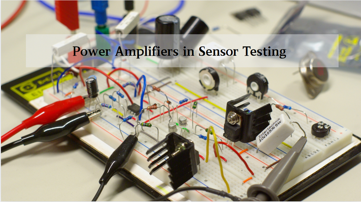
Multivariate Application Analysis of Power Amplifiers in Sensor Testing
In the field of modern sensor testing, power amplifiers (PAs) serve as core components and play an indispensable role. From amplifying weak signals to simulating complex physical environments, power amplifiers provide solid guarantees for the precise testing of sensor performance through their uniqu...
-
2025 / 06 / 28
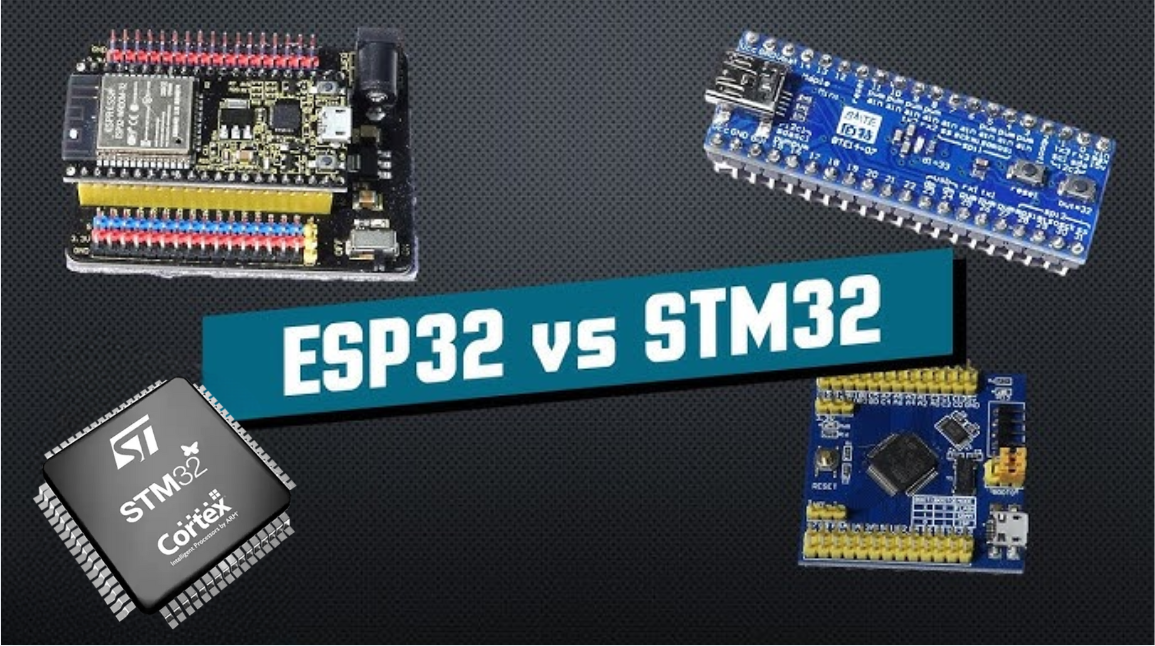
ESP32 vs STM32: Which Microcontroller Suits You Better?
In the field of embedded development, both ESP32 and STM32 are highly favored microcontrollers, each with unique features and advantages. When facing project development, how do you choose between them? This requires comprehensive consideration of multiple factors. The following detailed comparison ...
-
2025 / 06 / 26
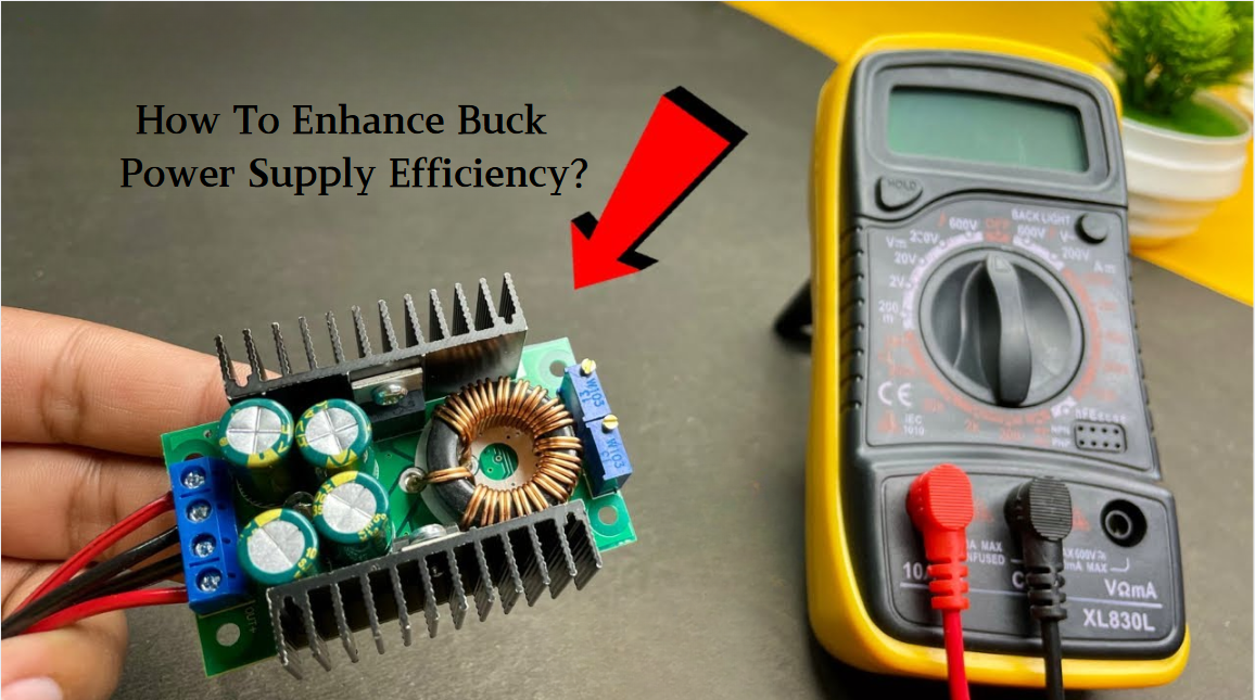
Key Strategies to Enhance Buck Power Supply Efficiency
Improving the efficiency of Buck (step-down) switching power supplies requires a multi-dimensional approach targeting energy loss sources, including component selection, topology optimization, control strategies, and thermal management. Below are core strategies and engineering practices:...
-
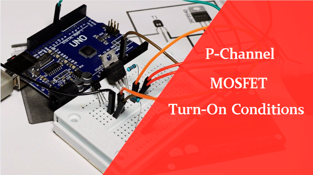
2025 / 06 / 26
P-Channel MOSFET Turn-On Conditions
The turn-on conditions for a P-channel MOSFET (PMOS) are inverse to those of an N-channel MOSFET (NMOS), primarily governed by the relationship between the gate-source voltage (VGS) and the threshold voltage (Vth), along with voltage polarity. Here are the key points:A PMOS turns on when its gate vo...
-
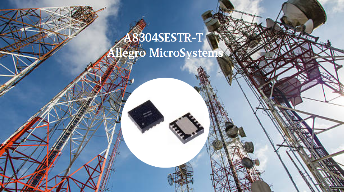
2025 / 06 / 24
A8304SESTR-T Allegro MicroSystems-Single LNB Supply and Control Voltage Regulator
The Allegro MicroSystems A8304SESTR-T is a single-channel Low Noise Block Regulator (LNBR). It integrates a monolithic boost converter with MOSFET, current sensing, and compensation. Featuring a 704 kHz switching frequency, it uses few external components. With an I²C-compatible interface, it offers...
-
2025 / 06 / 20
EG25GGC-128-SGNS by Quectel Wireless Solutions Co., Ltd: Features,Symbol,Footprint and Datasheet
The Quectel EG25GGC - 128 - SGNS is an LTE Cat 4 module optimized for M2M and IoT. Supporting 3GPP Rel. 11, it offers up to 150Mbps downlink and 50Mbps uplink. With global LTE/UMTS/GSM coverage, it's backward - compatible with EDGE/GPRS. Featuring multi - constellation GNSS (GPS, GLONASS, BeiDou, et...

-
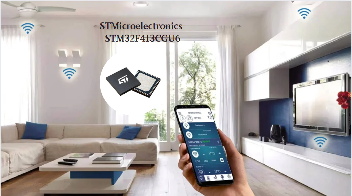
2025 / 06 / 17
STMicroelectronics STM32F413CGU6 Microcontroller: Datasheet, Performance, Features
The STMicroelectronics STM32F413CGU6 is an Arm® Cortex®-M4 based MCU with FPU, operating at up to 100 MHz for 125 DMIPS performance. It features 1MB Flash, 320KB SRAM, and interfaces like USB OTG FS, 3 CAN, ADC, 2 DAC, and multiple serial ports. With low-power modes (Sleep, Stop, Standby), it suits ...
-
2025 / 06 / 13
STMicroelectronics STM32F446ZCT6 -Microcontrollers: A Comprehensive Guide
The STMicroelectronics STM32F446ZCT6 is an ARM Cortex-M4-based MCU with FPU, running at up to 180 MHz. It features 256 KB Flash, 128 KB SRAM + 4 KB backup SRAM, and offers rich peripherals: USB OTG HS/FS, 2 CAN, 3 ADCs, 17 timers, and 20 communication interfaces. In LQFP144 package, industrial temp ...

-
2025 / 06 / 09
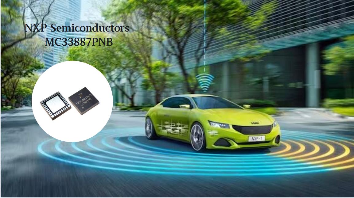
MC33887PNB NXP Semiconductors-Motor Drivers:A Comprehensive Guide
The NXP Semiconductors MC33887PNB is a 5.0 A H - bridge power IC with integrated load current feedback. It operates across a 5.0 V - 28 V voltage range, features low RDS(on) (120 mΩ typical), and supports up to 10 kHz PWM. With functions like active current limiting and fault reporting, it ensures r...
-
2025 / 06 / 07
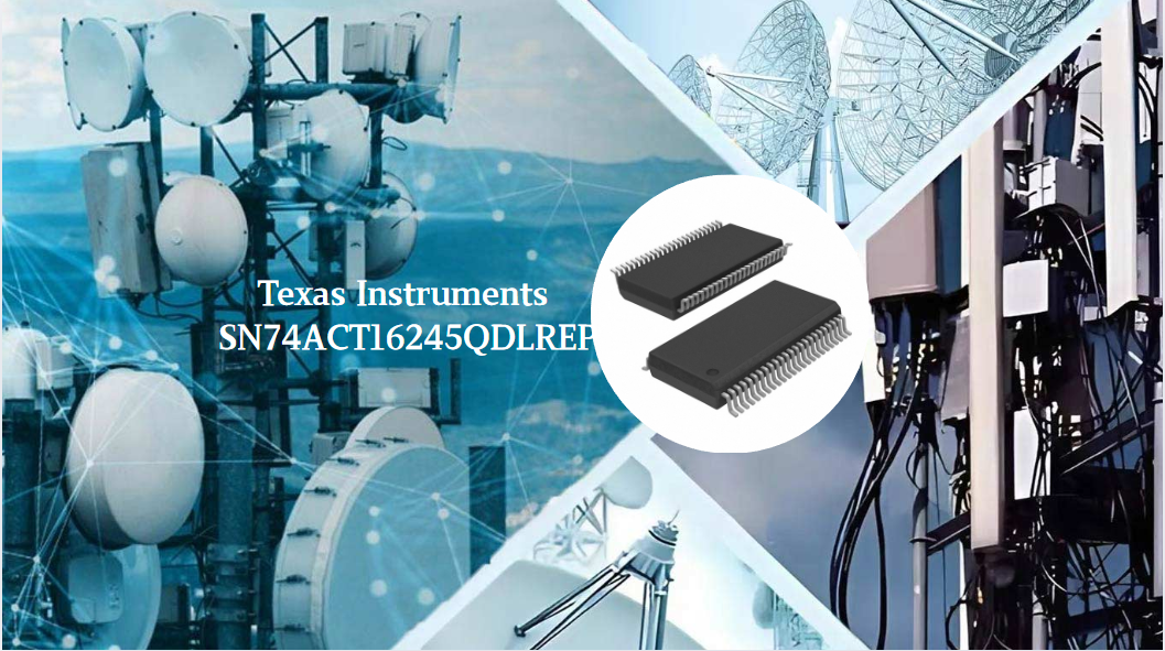
A 16-bit Bus Transceiver: Why Choose the Texas Instruments SN74ACT16245QDLREP?
The Texas Instruments SN74ACT16245QDLREP is a high-performance 16-bit bus transceiver. Designed for harsh industrial and automotive environments, it operates reliably from -40°C to +125°C. With its dual 8-bit non-inverting 3-state architecture, it enables efficient bidirectional data transfer. It of...

2000+
Daily average RFQ Volume

30,000,000
Standard Product Unit

2800+
Worldwide Manufacturers

15,000 m2
In-stock Warehouse
 Wishlist (0 Items)