

- RFQ
- BOM
-
Contact Us
Tel: +86-0755-83501315
Email: sales@sic-components.com


- Chinese
- English
- French
- German
- Portuguese
- Spanish
- Russian
- Japanese
- Korean
- Arabic
- Irish
- Greek
- Turkish
- Italian
- Danish
- Romanian
- Indonesian
- Czech
- Afrikaans
- Swedish
- Polish
- Basque
- Catalan
- Esperanto
- Hindi
- Lao
- Albanian
- Amharic
- Armenian
- Azerbaijani
- Belarusian
- Bengali
- Bosnian
- Bulgarian
- Cebuano
- Chichewa
- Corsican
- Croatian
- Dutch
- Estonian
- Filipino
- Finnish
- Frisian
- Galician
- Georgian
- Gujarati
- Haitian
- Hausa
- Hawaiian
- Hebrew
- Hmong
- Hungarian
- Icelandic
- Igbo
- Javanese
- Kannada
- Kazakh
- Khmer
- Kurdish
- Kyrgyz
- Latin
- Latvian
- Lithuanian
- Luxembou..
- Macedonian
- Malagasy
- Malay
- Malayalam
- Maltese
- Maori
- Marathi
- Mongolian
- Burmese
- Nepali
- Norwegian
- Pashto
- Persian
- Punjabi
- Serbian
- Sesotho
- Sinhala
- Slovak
- Slovenian
- Somali
- Samoan
- Scots Gaelic
- Shona
- Sindhi
- Sundanese
- Swahili
- Tajik
- Tamil
- Telugu
- Thai
- Ukrainian
- Urdu
- Uzbek
- Vietnamese
- Welsh
- Xhosa
- Yiddish
- Yoruba
- Zulu
- Kinyarwanda
- Tatar
- Oriya
- Turkmen
- Uyghur
Electronic Component Package Types
Electronic component package types serve as the interface between semiconductor devices and their application environments, ensuring mechanical protection, thermal management, and electrical connectivity. This article provides a detailed analysis of the most common packaging technologies, their applications, and the evolving trends shaping the industry.
1. Through-Hole Packaging
Dual In-line Package (DIP)
Structure: Features two parallel rows of pins extending from a rectangular plastic or ceramic body.
Applications: Legacy microcontrollers, timers (e.g., NE555), and early memory chips.
Advantages: Easy manual soldering, low cost, and compatibility with breadboard prototyping.
Limitations: Large footprint, limited pin count (typically ≤100), and low density.
Pin Grid Array (PGA)
Structure: Ceramic or plastic package with pins arranged in a grid pattern on the bottom.
Applications: High-performance CPUs (e.g., Intel Pentium Pro) and FPGAs.
Advantages: High pin count (up to 1,000+), excellent thermal dissipation.
Limitations: Requires socketed installation, high cost.
2. Surface Mount Technology (SMT)
Small Outline Package (SOP)
Structure: Thin, rectangular package with gull-wing leads on two sides.
Applications: Operational amplifiers (e.g., LM358), voltage regulators, and low-power ICs.
Advantages: Compact size, high density, and automated assembly.
Limitations: Limited pin count (≤40).
Quad Flat Package (QFP)
Structure: Square package with J-shaped or gull-wing leads on all four sides.
Applications: Microcontrollers, ASICs, and DSPs.
Advantages: High pin count (up to 208), fine pitch (0.5–0.8 mm).
Limitations: Sensitive to thermal stress, complex rework.
Quad Flat No-lead (QFN)
Structure: Leadless package with exposed thermal pad on the bottom.
Applications: Power management ICs, sensors, and RF modules.
Advantages: Ultra-compact, excellent thermal performance, and low parasitic inductance.
Limitations: Requires precise soldering.
Ball Grid Array (BGA)
Structure: Solder balls replace leads, arranged in a grid on the package bottom.
Applications: GPUs (e.g., NVIDIA RTX series), mobile processors (e.g., Apple A-series).
Advantages: High pin count (up to 4,000+), reduced signal noise, and improved thermal performance.
Limitations: Complex reflow soldering, high cost.
Chip Scale Package (CSP)
Structure: Package size ≤1.2× die size, with solder balls or leads.
Applications: Memory chips (e.g., DDR4), MEMS sensors, and cameras.
Advantages: Ultra-miniaturization, high I/O density.
Limitations: Sensitive to mechanical stress.
3. Advanced Packaging Technologies
Flip Chip
Structure: Chip is flipped and attached to the substrate using solder bumps.
Applications: High-speed processors, automotive ECUs, and AI accelerators.
Advantages: Short signal paths, high bandwidth, and improved thermal dissipation.
Limitations: Requires underfill material for reliability.
System-in-Package (SiP)
Structure: Multiple dies (e.g., CPU, memory, sensors) integrated into a single package.
Applications: Wearables (e.g., Apple Watch), 5G modules, and IoT devices.
Advantages: Reduced form factor, improved system performance, and design flexibility.
Limitations: Complex design and high manufacturing cost.
2.5D/3D Packaging
Structure: Dies are stacked vertically (3D) or placed on an interposer (2.5D).
Applications: High-performance computing (HPC), AI servers, and data centers.
Advantages: Ultra-high density, reduced latency, and improved power efficiency.
Limitations: Requires advanced materials (e.g., silicon interposers) and precision assembly.
Chiplet Technology
Structure: Complex chips are divided into smaller, reusable dies (chiplets) connected via advanced packaging.
Applications: AMD EPYC CPUs, Intel’s FPGA-based systems.
Advantages: Reduced design cost, improved yield, and scalability.
Limitations: Requires standardized interfaces (e.g., UCIe).
4. Packaging Materials and Environmental Considerations
Materials
Plastic: Cost-effective, widely used (e.g., SOP, QFP).
Ceramic: High thermal conductivity, hermetic sealing (e.g., PGA).
Metal: Excellent EMI shielding, used in military/aerospace.
Environmental Standards
RoHS Compliance: Restricts hazardous substances (e.g., lead, mercury) in packaging materials.
Lead-Free Soldering: Adopts Sn-Cu or Sn-Ag-Cu alloys to meet environmental regulations.
5. Key Trends and Future Directions
Miniaturization: Adoption of CSP and WLP for portable devices.
Heterogeneous Integration: SiP and Chiplet technologies enable multi-die systems.
Advanced Substrates: Glass interposers and organic materials for high-performance computing.
Sustainability: Development of eco-friendly materials and recycling processes.
Conclusion
Electronic component packaging is a critical enabler of modern electronics, balancing performance, reliability, and cost. From traditional DIP to cutting-edge 3D ICs, each package type addresses specific application needs. As technology evolves, advanced packaging will play a pivotal role in overcoming Moore’s Law limitations and driving innovation in AI, IoT, and HPC.
https://www.sic-components.com/category-all

Hot Products
View More-

1544443-2 TE Connectivity AMP Connectors
-
1544146-3 TE Connectivity AMP Connectors
-
1544256-1 TE Connectivity AMP Connectors
-
1544222-1 TE Connectivity AMP Connectors
-
1544425-2 TE Connectivity AMP Connectors
-
1544146-2 TE Connectivity AMP Connectors
-
1544200-1 TE Connectivity AMP Connectors
-
1544146-4 TE Connectivity AMP Connectors
-
1544207-1 TE Connectivity AMP Connectors
-
1544400-1 TE Connectivity AMP Connectors
-
1544174-1 TE Connectivity AMP Connectors
-
1544443-4 TE Connectivity AMP Connectors
Related Blogs
-
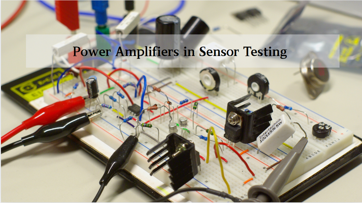
2025 / 06 / 30
Multivariate Application Analysis of Power Amplifiers in Sensor Testing
In the field of modern sensor testing, power amplifiers (PAs) serve as core components and play an indispensable role. From amplifying weak signals to simulating complex physical environments, power amplifiers provide solid guarantees for the precise testing of sensor performance through their uniqu...
-
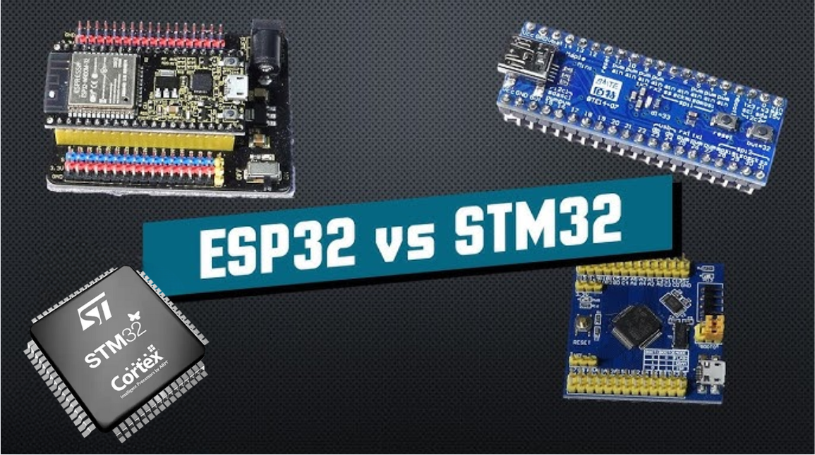
2025 / 06 / 28
ESP32 vs STM32: Which Microcontroller Suits You Better?
In the field of embedded development, both ESP32 and STM32 are highly favored microcontrollers, each with unique features and advantages. When facing project development, how do you choose between them? This requires comprehensive consideration of multiple factors. The following detailed comparison ...
-
2025 / 06 / 26
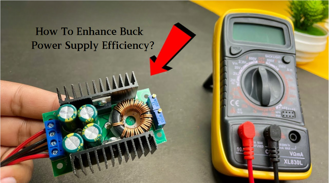
Key Strategies to Enhance Buck Power Supply Efficiency
Improving the efficiency of Buck (step-down) switching power supplies requires a multi-dimensional approach targeting energy loss sources, including component selection, topology optimization, control strategies, and thermal management. Below are core strategies and engineering practices:...
-
2025 / 06 / 26
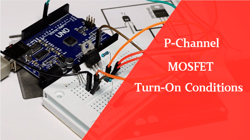
P-Channel MOSFET Turn-On Conditions
The turn-on conditions for a P-channel MOSFET (PMOS) are inverse to those of an N-channel MOSFET (NMOS), primarily governed by the relationship between the gate-source voltage (VGS) and the threshold voltage (Vth), along with voltage polarity. Here are the key points:A PMOS turns on when its gate vo...
-
2025 / 06 / 24
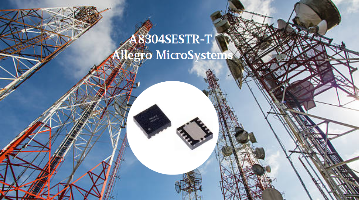
A8304SESTR-T Allegro MicroSystems-Single LNB Supply and Control Voltage Regulator
The Allegro MicroSystems A8304SESTR-T is a single-channel Low Noise Block Regulator (LNBR). It integrates a monolithic boost converter with MOSFET, current sensing, and compensation. Featuring a 704 kHz switching frequency, it uses few external components. With an I²C-compatible interface, it offers...
-
2025 / 06 / 20
EG25GGC-128-SGNS by Quectel Wireless Solutions Co., Ltd: Features,Symbol,Footprint and Datasheet
The Quectel EG25GGC - 128 - SGNS is an LTE Cat 4 module optimized for M2M and IoT. Supporting 3GPP Rel. 11, it offers up to 150Mbps downlink and 50Mbps uplink. With global LTE/UMTS/GSM coverage, it's backward - compatible with EDGE/GPRS. Featuring multi - constellation GNSS (GPS, GLONASS, BeiDou, et...

-
2025 / 06 / 17
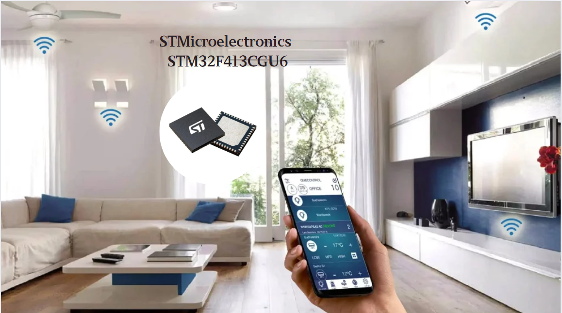
STMicroelectronics STM32F413CGU6 Microcontroller: Datasheet, Performance, Features
The STMicroelectronics STM32F413CGU6 is an Arm® Cortex®-M4 based MCU with FPU, operating at up to 100 MHz for 125 DMIPS performance. It features 1MB Flash, 320KB SRAM, and interfaces like USB OTG FS, 3 CAN, ADC, 2 DAC, and multiple serial ports. With low-power modes (Sleep, Stop, Standby), it suits ...
-
2025 / 06 / 13
STMicroelectronics STM32F446ZCT6 -Microcontrollers: A Comprehensive Guide
The STMicroelectronics STM32F446ZCT6 is an ARM Cortex-M4-based MCU with FPU, running at up to 180 MHz. It features 256 KB Flash, 128 KB SRAM + 4 KB backup SRAM, and offers rich peripherals: USB OTG HS/FS, 2 CAN, 3 ADCs, 17 timers, and 20 communication interfaces. In LQFP144 package, industrial temp ...

-
2025 / 06 / 09
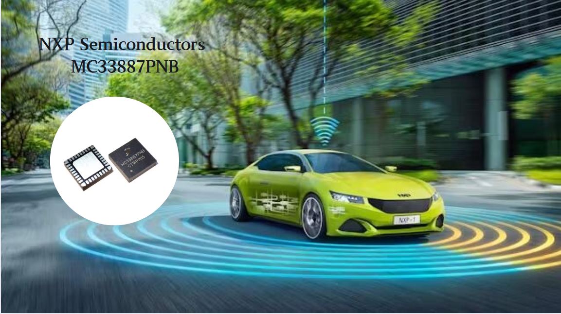
MC33887PNB NXP Semiconductors-Motor Drivers:A Comprehensive Guide
The NXP Semiconductors MC33887PNB is a 5.0 A H - bridge power IC with integrated load current feedback. It operates across a 5.0 V - 28 V voltage range, features low RDS(on) (120 mΩ typical), and supports up to 10 kHz PWM. With functions like active current limiting and fault reporting, it ensures r...
-
2025 / 06 / 07
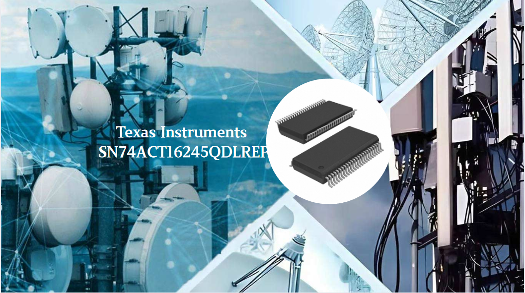
A 16-bit Bus Transceiver: Why Choose the Texas Instruments SN74ACT16245QDLREP?
The Texas Instruments SN74ACT16245QDLREP is a high-performance 16-bit bus transceiver. Designed for harsh industrial and automotive environments, it operates reliably from -40°C to +125°C. With its dual 8-bit non-inverting 3-state architecture, it enables efficient bidirectional data transfer. It of...

2000+
Daily average RFQ Volume

30,000,000
Standard Product Unit

2800+
Worldwide Manufacturers

15,000 m2
In-stock Warehouse
 Wishlist (0 Items)