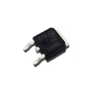
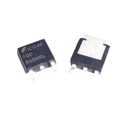
ONSemi/Fairchild FDD850N10L +BOM
The ONSemi/Fairchild FDD850N10L is an N-channel MOSFET designed for low/medium voltage applications. It features advanced trench technology for low on - resistance, reducing conduction losses. With fast switching speed and good avalanche ruggedness, it can handle voltage surges well. Its standardized package simplifies circuit design and it's suitable for various power management tasks.
ONSemi / Fairchild FDD850N10L's Features
1. Device Structure & Operation
- Enhancement-mode N-channel MOSFET for reliable switching and amplification in power circuits.
- Optimized for low gate charge and fast switching speeds, enabling efficient energy transfer in high-frequency applications.
2. Performance & Efficiency
- Low on-resistance (Rds(on)) to minimize conduction losses and improve overall system efficiency.
- High surge current capability for robust operation under transient load conditions.
3. Reliability & Robustness
- Built with advanced trench technology to enhance thermal stability and withstand harsh operating environments.
- Protection against common failure modes, such as thermal runaway and avalanche breakdown, for long-term reliability.
4. Applications & Design Flexibility
- Suitable for use in DC-DC converters, motor drives, battery management systems, and general power switching applications.
- Standard package (e.g., TO-220 or similar) for easy integration into existing circuit layouts.
5. Environmental & Compliance
- Lead-free and RoHS-compliant, adhering to international environmental standards.
- Halogen-free packaging (if applicable) for eco-friendly design requirements.
6. Gate Drive Requirements
- Low gate voltage drive capability, simplifying interface with common microcontroller or driver IC outputs.
ONSemi / Fairchild FDD850N10L's Applications
In the field of consumer appliances: In the power management circuits of products such as air conditioners, washing machines, and microwave ovens, the FDD850N10L can utilize its low on-resistance characteristic to reduce power consumption, improve the energy efficiency of the appliances, and achieve energy-saving effects. Its fast switching characteristic also helps to optimize the power conversion efficiency, stabilize the power supply, and ensure the stable operation of the appliances.
In the field of LED TVs and monitors: It is used in the power circuits of these devices to convert the input voltage into a stable voltage suitable for the LED backlight and the motherboard. The low gate charge and fast switching characteristics can reduce the energy loss during the switching process, improve the power conversion efficiency, and reduce power consumption. The low on-resistance can reduce the voltage drop during conduction, reduce heat generation, and enhance the stability of the device.
In the field of synchronous rectification: The FDD850N10L can play a crucial role in the synchronous rectification stage of the switching power supply. Due to its low on-resistance, it can significantly reduce the power loss during the rectification process and improve the power efficiency. The fast switching ability enables it to respond quickly to the signal changes in the circuit, accurately control the conduction and cut-off of the current, and ensure the efficient operation of synchronous rectification.
In the field of uninterruptible power supplies (UPS): In the power conversion circuit of the UPS, the avalanche test characteristic of the FDD850N10L enables it to maintain stable operation when facing sudden voltage changes, avoiding damage due to voltage fluctuations. The fast switching characteristic helps to achieve efficient power conversion, ensuring that when the mains power is interrupted, it can quickly switch to the backup power mode to continuously supply power to the devices.
In the field of micro solar inverters: In the micro solar inverters, the FDD850N10L is used to convert the direct current generated by the solar panels into alternating current. Its low on-resistance can reduce the energy loss, improve the conversion efficiency of the inverter, and enable more solar energy to be converted into usable electrical energy. The good dv/dt capability can effectively deal with the voltage fluctuations during solar power generation, ensure the stable operation of the inverter, and enhance the reliability of the photovoltaic power generation system.

ONSemi / Fairchild FDD850N10L's Attributes
| Series | PowerTrench® | Product Status | Active |
| FET Type | N-Channel | Technology | MOSFET (Metal Oxide) |
| Drain to Source Voltage (Vdss) | 100 V | Current - Continuous Drain (Id) @ 25°C | 15.7A (Tc) |
| Drive Voltage (Max Rds On, Min Rds On) | 5V, 10V | Rds On (Max) @ Id, Vgs | 75mOhm @ 12A, 10V |
| Vgs(th) (Max) @ Id | 2.5V @ 250µA | Gate Charge (Qg) (Max) @ Vgs | 28.9 nC @ 10 V |
| Vgs (Max) | ±20V | Input Capacitance (Ciss) (Max) @ Vds | 1465 pF @ 25 V |
| Power Dissipation (Max) | 50W (Tc) | Operating Temperature | -55°C ~ 175°C (TJ) |
| Mounting Type | Surface Mount | Supplier Device Package | TO-252AA |
| Package / Case | TO-252-3, DPAK (2 Leads + Tab), SC-63 | Base Product Number | FDD850 |
ONSemi / Fairchild FDD850N10L's Datasheet
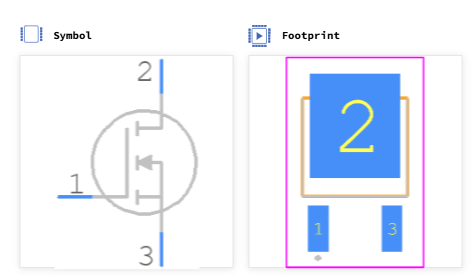
ONSemi / Fairchild FDD850N10L'sSymbol,Footprint and 3D Model

ONSemi / Fairchild FDD850N10L's Category-Low/Medium Voltage MOSFETs
In the modern trend of electronic systems pursuing efficiency, compactness, and reliability, Low/Medium Voltage MOSFETs (Metal-Oxide-Semiconductor Field-Effect Transistors) have emerged as critical hubs connecting power sources and loads, thanks to their superior voltage control capabilities and energy management advantages. Operating in the voltage range of low voltage (<50V) to medium voltage (50V to 400V), these power devices empower technological innovation across consumer electronics, industrial control, and new energy sectors through low losses, high-frequency response, and flexible adaptability, driving the global electronics industry toward greater efficiency and intelligence.
I. Core Technological Advantages of Low/Medium Voltage MOSFETs
The technical value of Low/Medium Voltage MOSFETs stems from the deep optimization of device structure and material processes:
1. Precise Voltage Control and Low Conduction Loss
The insulated gate design minimizes gate drive power to near-zero, enabling large-current switching with only a 微弱 voltage signal. Advanced trench technologies (such as Power Trench architecture) drastically reduce on-resistance, minimizing energy loss converted to heat and significantly improving power conversion efficiency—ideal for energy-sensitive portable devices and high-density power modules.
2. High-Frequency Switching and Stable Performance
Extremely low gate charge and reverse transfer capacitance grant nanosecond-level switching speeds, supporting high-frequency operation. Combined with excellent dv/dt tolerance, they suppress voltage spikes and electromagnetic interference (EMI), providing a stable signal environment for precision circuits. This is critical in high-frequency applications like wireless charging and LED lighting drivers.
3. Robust Design for Environmental Adaptation
Enhanced avalanche breakdown withstand capability and temperature stability allow these MOSFETs to handle voltage surges from inductive load switching (e.g., motor start/stop, relay operations) and wide-temperature fluctuations (-40°C to +125°C in industrial environments), ensuring long-term reliability under harsh conditions.
II. Diverse Applications Across Industries
The flexibility of Low/Medium Voltage MOSFETs makes them core components across sectors:
1. Consumer Electronics and Mobile Devices
In fast chargers for smartphones and laptop power adapters, their high-frequency switching enables smaller inductors and capacitors, driving miniaturization. In wearable devices like TWS earbuds and smartwatches, low quiescent power extends battery life, aligning with "lightweight and portable" design goals.
2. Industrial Control and Automation
As core components in motor drives, precise pulse-width modulation (PWM) supports fine-grained control of servo and stepper motor speed and torque, reducing mechanical vibration. In PLCs (Programmable Logic Controllers) and sensor interfaces, reliable switching ensures stable signal transmission, enhancing industrial automation levels.
3. New Energy and Green Technology
In distributed energy storage systems and micro solar inverters, they efficiently handle DC-DC conversion to reduce energy transfer losses. In electric vehicle battery management systems (BMS), they monitor battery status in real time and control charge/discharge loops, ensuring safe and efficient battery operation to boost EV range.
III. ONSemi/Fairchild FDD850N10L: A Benchmark for Low/Medium Voltage MOSFETs
As a classic product under ONSemi’s Fairchild brand, the FDD850N10L N-channel MOSFET integrates the core advantages of low/medium voltage devices, making it an ideal choice for efficient power management:
1. A Pinnacle of Energy Efficiency Optimization
Advanced trench technology achieves extremely low conduction losses, and fast switching enhances the efficiency of DC-DC converters and synchronous rectification circuits, reducing system heat—perfect for energy-critical consumer appliances and industrial power designs.
2. Reliability Across All Scenarios
Avalanche-resistant structures designed for complex electrical environments withstand voltage surges from inductive loads, ensuring stable long-term operation in applications like uninterruptible power supplies (UPS) and motor drives. RoHS-compliant lead-free technology meets global green design standards.
3. Simplified Design Integration
Standardized packaging (e.g., TO-220) enables seamless integration with existing circuit layouts, and low gate drive voltage requirements are compatible with mainstream microcontrollers and driver ICs, streamlining peripheral circuit design, shortening R&D cycles, and reducing overall costs.
From the miniaturization of consumer electronics to the high-reliability demands of industrial equipment, Low/Medium Voltage MOSFETs continue to address global needs for "efficiency, reliability, and sustainability" through technological breakthroughs. The ONSemi/Fairchild FDD850N10L, with its exceptional balance of loss control, reliability, and ease of use, not only provides proven efficiency solutions for traditional sectors but also demonstrates strong adaptability in emerging fields like IoT and new-energy vehicles. As the global electronics industry demands higher-performance power devices, these components will remain core building blocks, empowering engineers to create smarter and more efficient future electronic systems.
FDD850N10L's Manufacturers-ONSemi / Fairchild
ONSemi and Fairchild have achieved remarkable accomplishments in the field of Low/Medium Voltage MOSFETs (Metal-Oxide-Semiconductor Field-Effect Transistors).
Technological Innovation: They continuously explore new processes and architectures, leveraging advanced trench technology to drastically reduce on-resistance, thereby enhancing power conversion efficiency and minimizing energy loss. Their products feature extremely low gate charge and reverse transfer capacitance, enabling nanosecond-level switching speeds that support high-frequency operation while effectively suppressing electromagnetic interference (EMI).
Product Applications: Their MOSFETs are widely used across consumer electronics, industrial control, and new energy sectors. In consumer electronics, they facilitate the miniaturization of smartphone fast chargers and extend battery life in wearable devices. In industrial control, they enable precise motor control and stable signal transmission. In new energy applications, they optimize the efficiency of distributed energy storage systems and electric vehicle (EV) battery management.
Market Leadership: Renowned for superior performance and reliability, ONSemi/Fairchild products are the preferred choice for engineers globally. The classic FDD850N10L, for example, sets a performance benchmark with its low conduction losses, strong avalanche ruggedness, and ease of design integration, solidifying their position as industry leaders in low/medium voltage MOSFET solutions.
NVD6416ANT4G alternative parts: FDD850N10L
| Attributes |  |  |
| Part Number | NVD6416ANT4G +BOM | FDD850N10L +BOM |
| Manufacturer: | ON Semiconductor | ON Semiconductor |
| Description: | MOSFET N-CH 100V 17A DPAK | MOSFET 100V N-Channel PowerTrench MOSFET |
| Lifecycle Status: | LIFETIME (Last Updated: 1 week ago) | ACTIVE (Last Updated: 1 day ago) |
| Factory Lead Time: | 10 Weeks | 8 Weeks |
| Mounting Type: | Surface Mount | Surface Mount |
| Package / Case: | TO-252-3, DPak (2 Leads + Tab), SC-63 | TO-252-3, DPak (2 Leads + Tab), SC-63 |
| Surface Mount: | YES | - |
| Number of Pins: | 4 | 3 |
| Transistor Element Material: | SILICON | SILICON |
| Current - Continuous Drain (Id) @ 25℃: | 17A Tc | 15.7A Tc |
| Drive Voltage (Max Rds On, Min Rds On): | 10V | 5V 10V |
| Number of Elements: | 1 | 1 |
| Power Dissipation (Max): | 71W Tc | 50W Tc |
| Turn Off Delay Time: | 24 ns | 27 ns |
| Operating Temperature: | -55°C~175°C TJ | -55°C~175°C TJ |
| Packaging: | Tape & Reel (TR) | Tape & Reel (TR) |
| Published: | 2012 | 2010 |
| JESD-609 Code: | e3 | e3 |
| Pbfree Code: | yes | yes |
| Part Status: | Obsolete | Active |
| Moisture Sensitivity Level (MSL): | 1 (Unlimited) | 1 (Unlimited) |
| Number of Terminations: | 2 | 2 |
| ECCN Code: | EAR99 | EAR99 |
| Terminal Finish: | Tin (Sn) | Tin (Sn) |
| Terminal Form: | GULL WING | GULL WING |
| Pin Count: | 4 | - |
| Reference Standard: | AEC-Q101 | - |
| JESD-30 Code: | R-PSSO-G2 | R-PSSO-G2 |
| Element Configuration: | Single | Single |
| Operating Mode: | ENHANCEMENT MODE | ENHANCEMENT MODE |
| Power Dissipation: | 71W | 50W |
| Case Connection: | DRAIN |
Hot-selling products of SIC
71421LA55J8 UPD44165184BF5-E40-EQ3-A SST39VF800A-70-4C-B3KE IS66WV1M16DBLL-55BLI-TR AS4C32M16SB-7BIN Tags: FDD850N10L onsemi / Fairchild


 Wishlist (0 Items)