As one of the most representative integrated circuits in the 74LS series, the 74LS00, with its core design of four-channel 2-input NAND gates, has become a fundamental component in the field of digital electronics. This article will comprehensively analyze this classic chip.
74LS00 Overveiw
The 74LS00 is a widely used TTL (Transistor-Transistor Logic) integrated circuit that functions as a quad 2-input NAND gate. This means it contains four independent NAND gates, each with two input pins and one output pin. Each NAND gate in the 74LS00 performs the "NAND" logical operation: the output is low (logic 0) only when both of its inputs are high (logic 1); in all other cases (when at least one input is low), the output is high (logic 1). As a fundamental logic building block, it's essential for constructing more complex digital circuits like counters, flip-flops, and encoders, finding applications in various digital systems, industrial controls, and electronic devices.
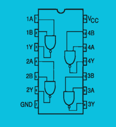
74LS00 Pinouts

| Pin No. | Pin Name | Description |
| NAND GATE 1 | ||
| 1 | A1 | Pin 1 will be the input of the first NAND gate in IC 74LS00. |
| 2 | B1 | Pin 2 will be used as the second Input of First NAND gate. |
| 3 | Y1 | The output of the first NAND gate will be available at Pin 3. |
| NAND GATE 2 | ||
| 4 | A2 | Pin 4 will be used for the input of the second NAND gate. |
| 5 | B2 | The second input of the second NAND gate will be given at Pin 5. |
| 6 | Y2 | The output of the second NAND gate will be available at Pin 6. |
| NAND GATE 3 | ||
| 9 | A3 | Pin 9 will be used as the first input pin for the third NAND gate. |
| 10 | B3 | Pin 10 will be the second input of the third NAND gate. |
| 8 | Y3 | Third NAND gate output will be at Pin 8. |
| NAND GATE 4 | ||
| 12 | A4 | Pin 12 will be used for the first input of the 4th NAND gate. |
| 13 | B4 | The second input of the fourth NAND gate will be at Pin 13. |
| 11 | Y4 | The output of the fourth NAND gate will available at Pin 11. |
| SHARED TERMINALS | ||
| 7 | GND | Pin 7 will be used at the common ground by devices and the power supply that will use with 74LS00. |
| 14 | Vcc | Pin 14 will be used to give power to the IC. |
74LS00 Specifications
| Type | Parameter |
| Operating Voltage Range | +4.75 to +5.25V |
| Maximum Supply Voltage | 7V |
| Maximum Output Current per Gate | 8mA |
| Output Type | TTL |
| Maximum ESD | 3.5KV |
| Typical Rise Time | 15ns |
| Typical Fall Time | 15ns |
| Operating Temperature Range | 0°C to 75°C |
| Pack/Case | SOIC, PDIP, and SOP. |
74LS00 Features
As a classic low-power Schottky TTL logic chip, the 74LS00 integrates performance, reliability, and flexibility. Here is a systematic summary of its core technical features:
Four independent channels design: Integrates four completely independent 2-input NAND gates, each capable of processing logic signals independently, supporting simultaneous implementation of four-channel logic functions (such as logic operations, signal buffering).
Standard pin compatibility: Adopts 14-pin Dual In-line Package (DIP) or surface-mount (SOIC/SOP) packaging, with a pin layout conforming to TTL standards (e.g., VCC connected to pin 14, GND to pin 7), facilitating direct cascading with other TTL chips.
Push-pull output structure: The output stage uses a push-pull design, providing strong driving capability, capable of outputting high levels (VOH ≥ 2.4V) and sinking large currents (maximum IOL of 8mA), suitable for directly driving loads such as LEDs and relays.
Wide power supply voltage range: Typical operating voltage is 5V, with an allowable fluctuation range of 4.75-5.25V and a limit value of 7V, adapting to different power supply environments.
TTL level compatibility: Input high-level threshold (VIH) ≥ 2V, low-level threshold (VIL) ≤ 0.8V, strictly following TTL standards; it also supports direct access to 3.3V or 2.5V logic signals (external level conversion required).
Medium-speed logic performance: Typical propagation delay (tpd) is 9-10ns, with a maximum data rate of 35Mbps, balancing speed and power consumption, suitable for most medium-speed digital circuit scenarios.
Low-power design: Static power consumption is only 9mW (typical value), much lower than earlier 74-series chips (e.g., 7400 is 40mW), suitable for long-running devices.
High sink current capability: Maximum low-level output current (IOL) is 8mA, capable of directly driving 10 LS-TTL loads or small peripherals (such as LED arrays) without additional buffers.
Advantages of push-pull output: The output stage adopts a push-pull structure, which can quickly pull up the level (VOH ≥ 2.4V) and efficiently sink current, reducing the risk of signal distortion, especially suitable for driving capacitive loads.
ESD protection: Built-in Electrostatic Discharge (ESD) protection circuit, capable of withstanding 3.5kV human-body model electrostatic shocks, enhancing long-term use stability.
Anti-noise capability: The input adopts a Schmitt trigger structure, with high noise margins (high-level noise margin VNH ≥ 0.4V, low-level VNL ≥ 0.4V), effectively suppressing signal interference.
Input protection mechanism: Unused input pins are recommended to be pulled up to VCC through a 1kΩ resistor or directly grounded to avoid false triggering caused by floating, ensuring logical stability.
Commercial grade (74LS00): Operating temperature range is 0-70°C, suitable for conventional scenarios such as consumer electronics and industrial control.
Military grade (54LS00): Extended to -55-125°C, meeting the needs of extreme environments such as aerospace and vehicle-mounted applications.
Storage stability: Storage temperature range is -65-150°C, with no impact on performance during long-term storage.
74LS00 Applications
Basic logic operations: In combinational logic circuits, it is not only used for simple "NAND" judgments (such as "triggering actions when two conditions are not met simultaneously") but also serves as a basic unit for signal inversion. For example, it performs logical inversion on control signals in data buses to switch between read and write instructions.
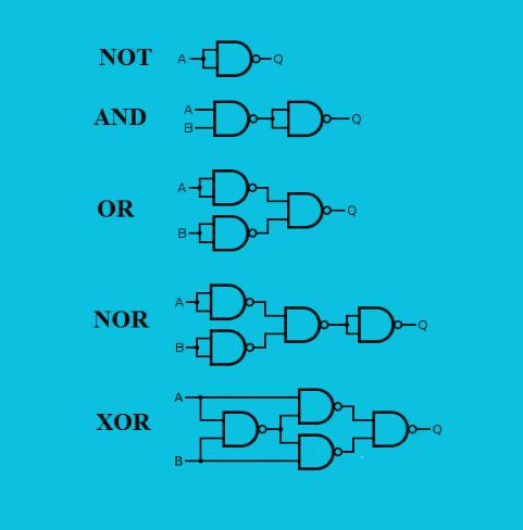
Universal gate conversion: With De Morgan's laws, shorting the two inputs can directly function as a NOT gate (single-input inversion); combining a NOT gate with a NAND gate forms an AND gate (eliminating the inverting characteristic of NAND); passing inputs through NOT gates first before connecting to a NAND gate results in an OR gate ![]() . This flexibility allows it to replace multiple dedicated gate chips, reducing circuit design complexity.
. This flexibility allows it to replace multiple dedicated gate chips, reducing circuit design complexity.
Storage and sequential circuits: SR flip-flops formed by cross-coupling two NAND gates can implement "set-reset" functions (such as state latching triggered by buttons); when extended to D flip-flops, they can synchronously store data under clock signal control, serving as core components of registers, shift registers, and counters (e.g., inter-bit logic connections in 4-bit binary counters).
Arithmetic circuits: In half-adders, NAND gates implement "XOR" (sum) and "AND" (carry) operations; full-adders handle carry propagation through cascaded NAND gates, widely used in addition modules of simple calculators; combined with inverting logic, they can realize binary subtraction (converted to addition via two's complement arithmetic), suitable for numerical processing in small digital instruments.
Industrial control and signal processing: In motor drive circuits, NAND gates judge multi-condition scenarios such as "emergency stop signal not triggered + start signal valid" to ensure safe startup; in sequential circuits, their fast switching characteristics are used for shaping sensor output pulse signals (eliminating glitches) or detecting rising/falling edges of clock signals, achieving precise timing synchronization (e.g., controlling trigger moments in data acquisition).
Educational and DIY scenarios: In electronic experiments, it is often used to demonstrate basic concepts such as truth table verification of logic gates and flip-flop latching principles; in DIY projects, it can build "dual-button unlock circuits" (unlocking only when both buttons are pressed) and "light-controlled + sound-controlled dual-condition lamps" (lighting up when it is dark and there is sound), enabling logic control without programming.
High-frequency and interface applications: Relying on TTL's nanosecond-level propagation delay (typically 10ns), it is suitable for peripheral interfaces of early computers (e.g., row-column signal decoding in keyboard scanning circuits) and baseband signal processing in short-distance communication (e.g., simple logic verification in UART protocols); its push-pull output can drive 10 standard TTL loads, allowing direct connection to peripherals like LEDs and relays, simplifying interface drive design.
Advantages of the 74LS00
The 74LS00 offers several key advantages that solidify its role as a foundational component in digital electronics:
Universal Logic Flexibility: As a quad 2-input NAND gate, it is a "universal gate"—easily reconfigurable into NOT, AND, OR, XOR, and other logic gates through simple wiring (leveraging De Morgan’s laws). This eliminates the need for multiple specialized ICs, simplifying circuit design and reducing component counts.
Strong TTL Compatibility: Operating on a standard +5V power supply and adhering strictly to TTL voltage standards (input/output levels), it integrates seamlessly with other TTL devices. This plug-and-play compatibility makes it a reliable choice in mixed TTL systems.
Balanced Performance: Its low-power Schottky (LS) design strikes a balance between speed and efficiency. With a typical propagation delay of ~10ns, it supports medium-to-high-speed applications, while its static power consumption (~9mW) is significantly lower than earlier 74-series variants (e.g., 7400 at 40mW), making it energy-efficient for long-running devices.
Robust Driving Capability: Equipped with a push-pull output stage, it can directly drive up to 10 standard TTL loads, avoiding the need for additional buffer circuits. This simplifies interfacing with peripherals like LEDs, relays, or other logic chips.
Practical Availability & Cost-Effectiveness: Widely available in 14-pin DIP (ideal for breadboard prototyping) and surface-mount packages, it is low-cost and easily sourced. This accessibility makes it a staple in educational labs, hobby projects, and small-scale production.
Reliability: Built-in ESD protection (withstanding 3.5kV human-body model discharges) and decent noise margins (≥0.4V for both high/low levels) enhance stability in noisy environments. Commercial-grade variants operate reliably at 0–70°C, with military-grade (54LS00) extending to -55–125°C for harsh conditions.
How to Use the 74LS00?
To use the 74LS00 (a quad 2-input NAND gate IC in the TTL family), follow these steps for setup, basic testing, and practical applications:
1. Hardware Setup: Power and Pinout
The 74LS00 requires a +5V DC power supply (TTL standard) and proper pin connections.
Step 1: Power Connections:
Connect pin 14 (Vcc) to +5V.
Connect pin 7 (GND) to the circuit’s ground.
- Strp 2: Pinout for 4 Independent NAND Gates:
The IC contains 4 separate 2-input NAND gates. Each gate has 2 inputs and 1 output:Gate Number Input A Input B Output Y 1 Pin 1 Pin 2 Pin 3 2 Pin 4 Pin 5 Pin 6 3 Pin 9 Pin 10 Pin 8 4 Pin 12 Pin 13 Pin 11
2. Basic Testing: Verify NAND Logic
The core rule of a NAND gate is: Output is LOW (0V) only if both inputs are HIGH (5V); otherwise, output is HIGH (5V).
Step 1: Build a Test Circuit
For one gate (e.g., Gate 1, pins 1, 2, 3):
- Connect input pins 1 and 2 to logic sources (e.g., toggle switches linked to +5V/GND, or breadboard rails).
- Connect output pin 3 to an indicator (e.g., an LED in series with a 220Ω resistor to GND; the LED lights when output is HIGH).
Step 2: Test All Input Combinations
Check if the output matches the NAND truth table:
| Input A (Pin 1) | Input B (Pin 2) | Expected Output (Pin 3) | LED State |
|---|---|---|---|
| 0V (LOW) | 0V (LOW) | 5V (HIGH) | ON |
| 0V (LOW) | 5V (HIGH) | 5V (HIGH) | ON |
| 5V (HIGH) | 0V (LOW) | 5V (HIGH) | ON |
| 5V (HIGH) | 5V (HIGH) | 0V (LOW) | OFF |
3. Advanced Use: Convert to Other Logic Gates
NAND gates are "universal"—they can mimic any logic gate with simple wiring:

Example 1: NOT Gate (Inverter)
A NOT gate inverts its input![]() :
:
- Wiring: Short the two inputs of a NAND gate (e.g., connect pin 1 to pin 2 of Gate 1).
- Logic:
 .
.
Example 2: AND Gate
An AND gate outputs HIGH only if both inputs are HIGH![]() :
:
Wiring:
Use Gate 1 as a NAND gate![]() .
.
Use Gate 2 as a NOT gate (short its inputs) to invert Gate 1’s output.
Connect Gate 1’s output (pin 3) to Gate 2’s inputs (pins 4 and 5).
Logic: ![]() .
.
Example 3: OR Gate
An OR gate outputs HIGH if at least one input is HIGH ![]() :
:
Wiring (using De Morgan’s law: ![]() :
:
Use two NAND gates as NOT gates (short their inputs) to create ![]() .
.
Connect ![]() to the inputs of a third NAND gate.
to the inputs of a third NAND gate.
Result: The third gate’s output equals A + B.
Key Precautions
Voltage Limits: Never exceed +7V on Vcc; inputs must stay within TTL levels (LOW: 0–0.8V; HIGH: 2–5V).
Decoupling: Add a 0.1μF capacitor between Vcc and GND to reduce power noise.
ESD Protection: Handle the IC carefully to avoid electrostatic damage.
Loads: Each output can drive up to 10 TTL loads. For heavier loads (e.g., relays), use a buffer.
74LS00 Alternative
SN54LS00: A military-grade version, it is fully functionally consistent with the 74LS00 (quad 2-input NAND gate), but features a wider operating temperature range (-55°C to 125°C) and higher reliability, making it suitable for extreme environments.
SN7400: An early standard TTL model in the 74 series, it is also a quad 2-input NAND gate but uses a non-Schottky process. It has higher power consumption than the LS series and slightly slower switching speed, while being compatible with basic TTL voltage levels.
CD4011: A quad 2-input NAND gate based on CMOS technology (part of the 4000 series). It has a wider operating voltage range (typically 3-18V) and extremely low power consumption, but its switching speed is slower than that of TTL. It is suitable for low-power scenarios and has the same logical function as the 74LS00.
74LS08: Belonging to the 74LS series, it functions as a quad 2-input AND gate (not a NAND gate) with a different logical operation—it outputs a high level only when both inputs are high. Attention should be paid to this functional difference.
74LS00CH/DC/J/N/NA/PC/W: All are derivative models of the 74LS00, with the same core function (quad 2-input NAND gate). The differences mainly lie in package types (such as DIP, SMD), manufacturer-specific markings, or quality grades. Their electrical parameters are compatible with the 74LS00, allowing direct interchangeability.
901521-01/AMX3550/C74LS00P/DM74LS00N, etc.: Most are equivalent models produced by various manufacturers (such as Texas Instruments, Hitachi, Toshiba, etc.). They are fully functionally consistent with the 74LS00 (quad 2-input NAND gate), with compatible pin configurations and electrical characteristics. They only differ due to manufacturers' naming conventions and can be directly substituted for use.
74LS00 vs. 74HC00
The 74HC00 and 74LS00 are both ICs featuring four basic NAND gates, which are fundamental in digital electronics. The key difference lies in their speed characteristics, with the 74HC00 being high-speed and the 74LS00 being low-speed.
Here are some other differences between the two ICs:
| Feature | 74LS00 | 74HC00 |
| Supported Voltage | Limited to 5V | 2V to 6V |
| Output Current (5V) | HIGH-Level Output Current: 0.4 mA; LOW-Level Output Current: 8 mA | 4 mA (sink or source) |
| Logic Levels | Standard TTL logic, 2.0 V@5Vcc for logic 1 | Hi logic level requires minimum 3.5 V@5Vcc |
| Output Drive | Higher output drive capability | - |
| Input Loading | Higher input loading | - |
| Speeds and Delays | Faster speeds, shorter delays | - |
| Compatibility | Not directly compatible due to differences in voltage levels and drive | Pin-compatible with 74LS00, but not directly compatible due to differences |
The HC family was designed to match the speed of the LS while consuming lower power, achieved through CMOS technology.
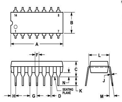
74LS00 Package Dimension

74LS00 Manufacturer
As a classic low-power Schottky TTL logic chip, the 74LS00 has a diversified landscape of manufacturers, encompassing multiple semiconductor giants from Europe, America, and Japan.
Fairchild Semiconductor is the pioneer of this chip. When it first launched the 74LS series in the 1970s, the 74LS00 became a cornerstone of digital circuits with its minimalist design of four 2-input NAND gates. Its DIP-14 package and push-pull output structure set industry standards.
Following closely, Texas Instruments (TI) strengthened its market leadership with the SN74LS00 series. Leveraging stable process control and military-grade (54LS00) product lines, it expanded applications into aerospace and industrial fields. National Semiconductor focused on the civilian market with its DM74LS00 series, emphasizing popularization in consumer electronics and educational scenarios.
Japanese manufacturers Hitachi and Renesas entered the Asia-Pacific market with the HD74LS00 series, offering SMD package versions to meet miniaturization needs. ON Semiconductor continued Motorola's production line, covering small and medium batch orders with high cost performance.
Notably, all manufacturers strictly adhere to the 14-pin TTL standard, ensuring direct interchangeability of 74LS00s from different brands. This open ecosystem has enabled its continuous application for over half a century. Today, while TI and ON Semiconductor remain mainstream suppliers, Fairchild's technical legacy as the pioneer is forever etched in the genes of this "universal building block of digital circuits."
Conclusion
In summary, with its stable NAND gate logic function, electrical characteristics compatible with TTL levels, and wide adaptability to scenarios, the 74LS00 has become an indispensable basic component in digital circuit design.
If you need to obtain the latest quotation and supply chain information for this series of chips, please feel free to contact us at any time, and we will provide you with professional technical support and procurement services.


 Wishlist (0 Items)