The LT3097 is a dual, positive and negative, high-performance, low-dropout linear regulator featuring Analog Devices, Inc., ultralow noise and ultra-high power supply rejection ratio (PSRR) architecture for powering noise-sensitive applications. Each regulator delivers up to 500 mA with a typical 260 mV/235 mV (positive/negative) dropout voltage.
Operating quiescent current is nominally 2.2 mA/2.35 mA (positive/negative) and drops to 0.3 μA/3 μA (positive/negative) in shutdown. The LT3097 has a wide output voltage range (0 V to 15 V, positive and 0 V to -19.5 V, negative) error amplifier that operates in unity-gain and provides virtually constant output noise, PSRR, bandwidth and load regulation, independent of the programmed output voltage.
LT3097 is stable with a minimum 10 μF ceramic output capacitor for each channel. Built-in protection includes internal current limit with foldback and thermal limit with hysteresis. The positive regulator also includes reverse-battery protection and reverse-current protection. The LT3097 is available in a thermally enhanced, 22-lead 6 mm × 3 mm, Plastic dual-flat no-leads (DFN) package.
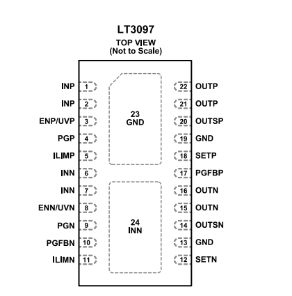
LT3097 Pinout

![]()
| Pin No. | Mnemonic | Description |
|---|---|---|
| 1, 2 | INP | Positive input terminal, supplies power to the positive regulator. A bypass capacitor (recommended ≥4.7µF) is required to suppress noise. It supports reverse voltage protection (no reverse current when the battery is connected in reverse). |
| 3 | ENP/UVP | Positive channel enable/undervoltage lockout (UVLO) pin: Pulling low puts the positive regulator into shutdown mode (quiescent current < 1µA); The UVLO threshold can be set via a resistor divider (turn-on voltage 1.24V, hysteresis 130mV); Connect to INP if unused, do not float. |
| 4 | PGP | Positive power good flag (open-collector), indicates status when the output voltage is stable; Pulls low when PGFBP < 300mV; Disabled in shutdown mode, avoid driving more than 0.3V below GND. |
| 5 | ILIMP | Positive channel current limit programming pin: External resistor to GND sets the maximum current (scaling factor 150mA×kΩ); Can monitor output current (1:500 ratio, voltage 0~300mV); Connect to GND if unused, do not float. |
| 6, 7 | INN | Negative input terminal, supplies power to the negative regulator. A bypass capacitor is required, and it is connected to EPAD (INN) to enhance stability. |
| 8 | ENN/UVP | Negative channel enable/undervoltage lockout pin, functions the same as ENP/UVP, controls the shutdown/turn-on of the negative regulator and UVLO threshold setting. |
| 9 | PGN | Negative power good flag, functions the same as PGP, indicates the regulation status of the negative output voltage, avoid driving more than 0.3V below GND. |
| 10 | ILIMN | Negative channel current limit programming pin, functions the same as ILIMP, sets the maximum current of the negative channel and monitors the output current. |
| 11 | SETN | Negative output voltage programming pin, external resistor to GND precisely adjusts the negative output voltage (0~-19.5V), with SET current accuracy of ±1%. |
| 12 | OUTSN | Negative output sense terminal, serves as the non-inverting input of the negative regulator's error amplifier. Kelvin connect to the output capacitor and load to optimize performance, avoid driving more than 0.3V below GND. |
| 13, 14 | OUTN | Negative output terminal, provides adjustable voltage of 0~-19.5V. A ≥10µF ceramic capacitor (ESR < 20mΩ) is required to ensure stability, supporting 500mA output current. |
| 15 | GND | Ground pin, provides a reference potential for the circuit, connected to EPAD (GND) to enhance grounding performance. |
| 16 | SETP | Positive output voltage programming pin, external resistor to GND precisely adjusts the positive output voltage (0~15V), with SET current accuracy of ±1%. |
| 17 | PGFBP | Positive channel feedback compensation terminal, external capacitor optimizes loop stability and affects PGP logic judgment. |
| 18 | PGFBN | Negative channel feedback compensation terminal, external capacitor optimizes negative channel loop stability and affects PGN logic judgment. |
| 19 | GND | Main ground pin, connected to EPAD (GND) to ensure low-impedance grounding. |
| 20 | OUTSP | Positive output sense terminal, serves as the non-inverting input of the positive regulator's error amplifier. Kelvin connect to the output capacitor and load to optimize transient performance, avoid driving more than 0.3V below GND. |
| 21, 22 | OUTP | Positive output terminal, provides adjustable voltage of 0~15V. A ≥10µF ceramic capacitor (ESR < 20mΩ, ESL < 2nH) is required to ensure stability, supporting 500mA output current. |
| 23 | EPAD (GND) | Exposed ground pad, connected to GND pins, soldered to the PCB ground plane to enhance heat dissipation and electrical performance. |
| 24 | EPAD (INN) | Exposed INN pad, connected to INN pins, improves the power supply stability and heat dissipation capability of the negative channel. |
LT3097Absolute Maximum Ratings
| Parameter | Value |
|---|---|
| INP Pin Voltage | ±22 V |
| INN Pin Voltage | with Respect to GND Pin –22 V to +0.3 V |
| ENP/UVP Pin Voltage | ±22 V |
| ENN/UVN Pin Voltage | with Respect to INN Pin¹ –0.3 V to +30 V with Respect to GND Pin ±22 V |
| INP-to-ENP/UVP Differential | ±22 V |
| PGP Pin Voltage² | –0.3 V, +22 V |
| PGN Pin Voltage | with Respect to INN Pin¹ –0.3 V to +30 V with Respect to GND Pin –0.3 V to +22 V |
| ILIMP Pin Voltage² | –0.3 V, +1 V |
| ILIMN Pin Voltage | with Respect to INN Pin¹ –0.3 V to +22 V |
| PGFBP Pin Voltage² | –0.3 V, +22 V |
| PGFBN Pin Voltage | with Respect to INN Pin¹ –0.3 V to +30 V with Respect to GND Pin ±22 V |
| SETP Pin Voltage² | –0.3 V, +16 V |
| SETP Pin Current³ | ±20 mA |
| SETN Pin Voltage | with Respect to INN Pin¹ –0.3 V, +22 V with Respect to GND Pin ±22 V |
| SETN Pin Current⁴ | ±10 mA |
| OUTSP Pin Voltage² | –0.3 V, +16 V |
| OUTSP Pin Current³ | ±20 mA |
| OUTSN Pin Voltage | with Respect to INN Pin¹ –0.3 V, +22 V with Respect to GND Pin ±22 V |
| OUTSN Pin Current⁴ | ±10 mA |
| SETN-to-OUTSN Differential⁵ | ±22 V |
| OUTP Pin Voltage² | –0.3 V, +16 V |
| OUTN Pin Voltage | with Respect to INN Pin¹ –0.3 V, +22 V with Respect to GND Pin ±22 V |
| OUTP-to-OUTSP Differential⁶ | ±1.2 V |
| OUTN-to-OUTSN Differential⁷ | ±22 V |
| INP-to-OUTP Differential | ±22 V |
| INP-to-OUTSP Differential | ±22 V |
| Output Short-Circuit Duration | Indefinite |
| Temperature | Operating TJ Range⁸, A Grade –40°C to +125°C Storage Range –65°C to +150°C |
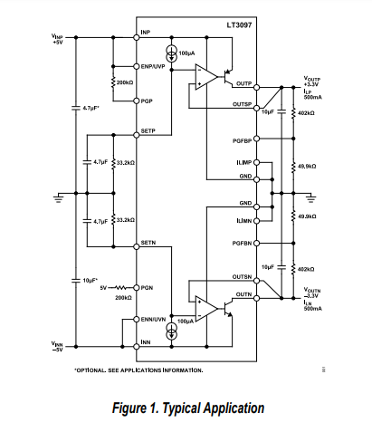
LT3097Typical Application Circuit

The typical application circuit of LT3097 uses this linear voltage regulator as the core to build a dual positive - negative output system. The circuit connects to positive and negative power supplies (V₊, V₋). By cooperating with resistors like 200kΩ, 420kΩ and capacitors such as 4.7μF, 1nF, and leveraging the precise regulation of LT3097, it achieves a stable output of +2.27V and -2.27V (both at 500mA). Suited for low - noise, high - precision power supply needs, it can be applied in scenarios like analog signal chains and precision instruments. Through the synergy of components, it ensures voltage stability and anti - interference capability, serving as a typical solution for high - performance power supply design.
LT3097 Featrues
Ultra-low output RMS noise: 0.8 μV rms (10 Hz to 100 kHz)
Ultra-low output noise spectral density: 2 nV/√Hz (Positive) and 2.2 nV/√Hz (Negative) at 10 kHz
Ultra-low 1/f noise: 10 μV p-p (Positive) and 3.2 μV p-p (Negative) (0.1 Hz to 10 Hz)
Ultra-high PSRR: 76 dB (Positive) and 74 dB (Negative) at 1 MHz
Output current: 500 mA
Wide input voltage range: ±1.8 V to ±20 V
Single capacitor per channel improves noise and PSRR
SET pin current: 100 μA, ±1% initial accuracy
Single resistor per channel programs output voltage
Programmable current limit
Low-dropout voltage: 260 mV (Positive) and 235 mV (Negative)
Output voltage range: 0 V to 15 V (Positive) and 0 V to –19.5 V (Negative)
Programmable power good
Fast start-up capability
Precision enable/undervoltage lockout (UVLO)
Internal current limit with foldback
Minimum output capacitor: 10 μF ceramic
Compact, low-profile, 22-lead, 6 mm × 3 mm, Plastic DFN package
LT3097 Applications
The LT3097 delivers exceptional value in scenarios demanding high-quality power.
Bipolar very low-noise power supplies: It provides ultra-low noise (0.8μV RMS positive, 2.2nV/√Hz negative) for noise-sensitive bipolar circuits like precision op-amps, ensuring stable ±0-15V/+0 to -19.5V outputs.
RF power supplies: With ultra-high PSRR (76dB/74dB at 1MHz) and low 1/f noise, it supports PLLs, VCOs, mixers, and amplifiers by suppressing interference.
Low-noise instrumentation: Unity-gain architecture minimizes noise for spectrum analyzers and sensors, enabling nanoscale measurements.
Data converters: Low dropout (260mV/235mV) and fast startup reduce errors in high-speed ADCs/DACs, boosting ENOB and dynamic range.
Medical applications:Its stability enhances MRI/CT clarity and ECG accuracy, aiding early diagnosis.
Precision power supplies: ±1% SET pin accuracy and low regulation enable precise voltage programming for lab references.
Switching supply postregulation: Ultra-high PSRR suppresses 100kHz-1MHz noise, combining efficiency with low noise for sensitive circuits.

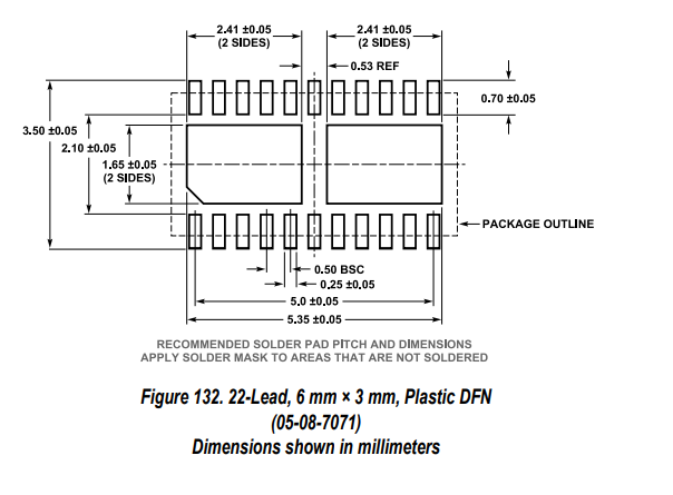
LT3097 Package

The LT3097 adopts a 22 - lead, 6 mm × 3 mm plastic DFN (Dual - Flat No - leads) package. As shown in the diagram, it has a compact outline. The overall dimensions are precisely defined, with parameters like length (5.35 ± 0.05 mm), width (3.50 ± 0.05 mm), etc. The recommended solder pad pitch and dimensions ensure proper soldering. This package offers a low - profile, space - saving solution, beneficial for high - density circuit designs, while also facilitating thermal management and electrical performance in applications requiring high - precision power regulation.
LT3097 vs. Other Voltage Regulators
| Feature | LT3097 | LT1763 | TPS7A4700 |
|---|---|---|---|
| Output Current | 500 mA | 500 mA | 1 A |
| Output Voltage Range | 0.6V–19.5V | 1.22V–20V | 1.4V–20.5V |
| Output Noise | 0.8 μVRMS | 20 μVRMS | 4 μVRMS |
| PSRR @ 1 kHz | 76 dB | 60 dB | 66 dB |
| Dropout Voltage | 250 mV | 300 mV | 200 mV |
LT3097 Manufacturer
The LT3097 is manufactured by Analog Devices, Inc. (ADI), a global leader in high - performance analog, mixed - signal, and digital signal processing (DSP) integrated circuits. ADI has a long - standing reputation for innovation and quality in the semiconductor industry. Since its founding, it has been dedicated to developing cutting - edge technologies that address the challenges of modern electronics. The company's products are widely used in various fields, including industrial automation, communications, healthcare, and automotive. When it comes to the LT3097, ADI leverages its deep expertise in analog design. The company's state - of - the - art manufacturing facilities and rigorous quality control processes ensure that the LT3097 meets the high standards of low noise, high power - supply rejection ratio (PSRR), and stable voltage regulation, making it a preferred choice for applications demanding precise power management.
LT3097 Categroy-low-dropout linear regulator
Low-dropout linear regulators (LDOs) are critical in power management, providing stable output voltages with minimal voltage difference between input and output (dropout voltage). This feature lets them operate efficiently even when input voltage is close to the desired output, ideal for battery-powered devices or systems with tight voltage margins. LDOs excel in noise-sensitive applications due to their ability to suppress input noise, ensuring clean power for sensitive components like sensors or RF circuits. Key parameters include dropout voltage, noise levels, power supply rejection ratio (PSRR), and load regulation, which determine their suitability for precision tasks. Among high-performance LDOs, the LT3097 stands out. With ultra-low dropout (260mV for positive, 235mV for negative channels) and exceptional noise suppression, it’s tailored for demanding scenarios, merging LDO advantages with bipolar output capability to meet strict power quality needs.
Conclusion
LT3097 is a high-performance linear voltage regulator focused on high-precision power management. Leveraging precise dual-channel voltage regulation (stably delivering ±2.27V/500mA), low-noise operation, and strong anti-interference capabilities, it serves as a core solution for scenarios demanding ultra-pure power supplies—such as analog signal chains, precision instruments, and high-end test & measurement equipment.
By cooperating with peripheral components, it effectively ensures voltage stability, suppresses noise interference, and directly boosts system signal accuracy and long-term operational reliability—acting as a key enabler for power supply design in high-performance electronic systems.
If you need to purchase LT3097 or obtain quotes for products in this series, please contact us!
Hot-selling products of SIC
71421LA55J8 UPD44165184BF5-E40-EQ3-A SST39VF800A-70-4C-B3KE IS66WV1M16DBLL-55BLI-TR AS4C32M16SB-7BIN W25Q16FWSNIG
AS7C34098A-20JIN 752369-581-C W957D6HBCX7I TR IS61LPS12836EC-200B3LI MX25L12875FMI-10G QG82915PL
Product information is from SIC Electronics Limited. If you are interested in the product or need product parameters, you can contact us online at any time or send us an email: sales@sic-chip.com.


 Wishlist (0 Items)