The LatticeXP2 Family is a series of low - cost, third - generation, non - volatile FPGAs. Based on the unique flexiFLASH architecture, it combines 4 - input Look - up Table (LUT) based FPGA fabric with non - volatile Flash cells. This architecture enables instant - on (in just 1ms), single - chip integration, and offers features like high logic - to - I/O ratio, embedded and distributed memory, and flexible, high - performance I/Os. LatticeXP2 devices support Live Update technology with TransFR, which allows for logic configuration updates during system operation. They also feature 128 - bit AES bitstream encryption and Dual Boot technologies for enhanced security and reliability. With densities ranging from 5K to 40K LUTs, these FPGAs can meet various design requirements. The family comes with high - performance sysDSP blocks, up to 4 sysCLOCK PLLs, and versatile I/O buffers that support multiple standards. The Lattice ispLEVER design tool, along with pre - designed IP modules, helps designers implement complex designs efficiently. The Brevia Development Kit provides a convenient platform for evaluation and design, making the LatticeXP2 Family suitable for a wide range of applications.

LatticeXP2 Family's Features
The LatticeXP2 Family is a series of FPGAs with multiple advanced features, making it suitable for various applications. Here are its key features:
- flexiFLASH Architecture
- Instant - on and Single - chip Integration: Achieves instant - on in 1ms and enables single - chip integration, which is convenient for system design and reduces the complexity of the overall circuit.
- High Logic - to - I/O Ratio: Offers a high ratio, allowing for efficient utilization of logic resources while handling a relatively large number of input/output signals.
- Embedded & Distributed Memory: Provides both embedded and distributed memory. The embedded sysMEM EBR can reach up to 885 Kbits, and the distributed RAM can reach up to 83 Kbits, meeting different data storage requirements in designs.
- Flexible, High - performance I/Os: The versatile I/Os support standards like DDR/DDR2 and 7:1 LVDS, and the sysIO buffer supports multiple voltage levels such as LVCMOS, SSTL, HSTL, PCI, LVDS, etc., ensuring compatibility with various external devices.
- Live Update Technology
- TransFR Technology: Allows for logic configuration updates while the equipment is still operating, enabling seamless system upgrades without the need for system downtime.
- Dual Boot with External SPI Flash: Improves system reliability. In case of a problem with one boot image, the system can still boot from the other, ensuring continuous operation.
- Secure Updates with 128 - bit AES Bitstream Encryption: Ensures the security of design data during updates. A 128 - bit AES encryption algorithm and a design - specific key stored in on - chip Flash protect the bitstream from being tampered with.
- Optimized FPGA Architecture
- Density Options: Available with densities ranging from 5K to 40K 4 - input Look - up Tables (LUTs), suitable for designs with different complexity requirements, from simple to complex.
- Memory Resources: In addition to the aforementioned memory, it offers a large amount of block RAM and distributed RAM, which is beneficial for data - intensive applications.
- Low - cost Packaging: Comes in low - cost TQFP, PQFP, and BGA packaging options, reducing the overall cost of the design while maintaining performance.
- High - Performance sysDSP Block
- Multiple Blocks and Multipliers: Equipped with three to eight blocks with multiply - and - accumulate functions, and contains 12 to 32 18x18 multipliers. Each block also supports different multiplier configurations like one 36x36 multiplier, four 18x18 multipliers, or eight 9x9 multipliers, providing flexibility for digital signal processing tasks.
- Pre - engineered Source Synchronous Interfaces
- High - speed Interfaces: The DDR/DDR2 interfaces can reach up to 200MHz/400Mbps, the 7:1 LVDS interface can reach up to 600Mbps, and the generic interface can reach up to 750Mbps, enabling fast data transfer in applications such as high - speed data communication and video processing.
- System - level Support
- Programming and Testing Interfaces: Features SPI/JTAG interfaces for device programming and complies with IEEE Standard 1149.1 Boundary Scan for easy testing and debugging.
- On - board Oscillator: An on - board oscillator is provided for initialization and general - purpose use, reducing the need for external components.
- Soft Error Detect (SED) Logic: Embedded SED logic helps to detect soft errors, enhancing the system's reliability in the presence of external interference.
- Power Supply: Operates with a 1.2V power supply core voltage, which is suitable for low - power - consumption designs
LatticeXP2 Family's Architecture
- Core Advantages of the flexiFLASH Architecture: The unique flexiFLASH architecture innovatively combines the FPGA fabric based on 4-input Look-up Tables (LUTs) with non-volatile Flash cells. This architecture enables a fast 1ms instant-on and supports single-chip integration, enhancing the compactness and reliability of the system. Meanwhile, it has a high logic-to-I/O ratio, which can efficiently handle a large number of logic operations and data transfer tasks. The architecture also provides distributed and embedded memory. The sysMEM embedded block RAM (EBR) can reach up to 885 Kbits, and the distributed RAM can be up to 83 Kbits, meeting different data storage and processing requirements.
- Collaborative Work of Abundant Functional Modules
- High-performance sysDSP Modules: These modules contain 3 - 8 blocks with multiply-and-accumulate functions and 12 - 32 18x18 multipliers. Each block also supports multiple multiplier configurations, such as one 36x36 multiplier, four 18x18 multipliers, or eight 9x9 multipliers. They perform outstandingly in digital signal processing and can be widely applied in fields like image and audio processing.
- sysCLOCK PLL Modules: Each device is equipped with up to 4 analog Phase Locked Loops (PLLs), which can achieve clock multiplication, division, and phase-shifting functions. They provide stable and precise clock signals for the system, ensuring the synchronous and efficient operation of each module.
- Flexible sysIO Buffers: The sysIO buffers support multiple voltage levels, such as LVCMOS 3.3/2.5/1.8/1.5/1.2, LVTTL, SSTL, HSTL, PCI, LVDS, etc., enabling good compatibility with various external devices and meeting different interface requirements.
- Pre-engineered Source Synchronous Interfaces: These interfaces support DDR / DDR2 interfaces with a maximum frequency of 200MHz and a data transfer rate of 400Mbps. The 7:1 LVDS interface has a maximum rate of 600Mbps, and the generic interface can reach 750Mbps, ensuring high-speed data transmission and being suitable for applications with high bandwidth requirements, such as video transmission.
- Complete System-level Support: It has SPI/JTAG interfaces for device programming and debugging, conforms to the IEEE Standard 1149.1 Boundary Scan standard, which is convenient for system testing. The on-chip oscillator is used for initialization and general purposes, reducing the dependence on external clock sources. In addition, Soft Error Detect (SED) logic is embedded to enhance system stability. The operating power supply voltage is 1.2V, which helps to achieve a low-power consumption design.
LatticeXP2 Family's Applications
The LatticeXP2 series, with its rich features, has a wide range of applications in multiple fields:
Video Processing Field: Its high-speed 7:1 LVDS interface enables fast transmission of image data, making it suitable for video applications. For example, in high-definition video surveillance systems, it can efficiently transmit a large amount of image data collected by cameras, ensuring the smoothness and real-time performance of videos. In video display devices, it can quickly transmit processed video signals to the display panel, supporting the display of high-resolution and high-frame-rate videos.
Industrial Control Field: This series has the feature of instant startup (1ms), which is crucial for the rapid response of key control logic in industrial control systems. For instance, in the control system of an automated production line, it can start up quickly and monitor and control the equipment status in real time, improving production efficiency and the stability of the system. In addition, it supports flexible sysIO buffers with multiple level standards and pre-designed source synchronous interfaces, making it convenient to connect with various industrial sensors, actuators and other devices, meeting the complex communication requirements of industrial sites.
Communication Field: It supports DDR/DDR2 interfaces, with a maximum frequency of up to 200MHz and a data transmission rate of 400Mbps, and the general interface rate can reach 750Mbps. It can be applied to the data processing and transmission links in communication devices. For example, in network switches, routers and other devices, it can efficiently process a large number of data packets, ensuring the high speed and stability of network communication. At the same time, the on-chip integrated resources, such as the sysDSP module and PLL, can be used for signal processing and clock management, enhancing the performance of communication devices.
Embedded System Field: The LatticeMico32™ soft processor enables the LatticeXP2 to be used as a microcontroller, providing more options for embedded system development. Combining its rich logic and signal processing resources, as well as flexible I/O interfaces, in embedded devices such as smart homes and smart electricity meters, it can implement complex control functions and data processing tasks. Moreover, with the advantage of single-chip integration, it reduces the size and cost of the devices.
Internet of Things (IoT) Field: The LatticeXP2 supports the Live Update technology, which can update the logic configuration while the device is running, facilitating the remote upgrade and function optimization of IoT devices. Meanwhile, the 128-bit AES encryption technology ensures the security of data transmission and storage, meeting the strict security requirements of IoT devices. In IoT sensor nodes, its low-power consumption and small size features can be utilized to achieve long-term operation and efficient data collection, processing and transmission.
Brevia Development Kit
Kit Overview
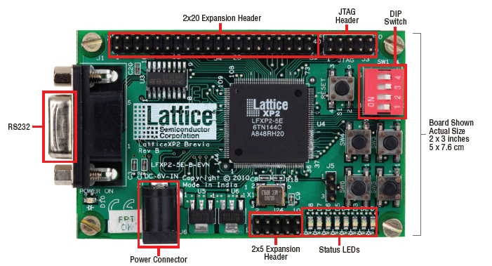
The Brevia Development Kit is an easy - to - use and low - cost platform for evaluating and designing with LatticeXP2 FPGAs. It provides developers with a complete set of resources, aiming to accelerate the development process and reduce development costs.

Main Components
Kit Advantages
The kit enables developers to quickly evaluate the performance and functions of the LatticeXP2 FPGA with a low - cost investment. With the help of free design tools, rich reference designs, and ready - made SoC demos, developers do not need to build basic functions from scratch. Instead, they can focus on the unique parts of their designs, improving development efficiency and accelerating the time - to - market of products.
Brevia Development Kit Products
LFXP2-5E-B2-EVN LFXP2-17E-L-EVN LFXP2-17E-H-EVN LFXP2-8E-7TN144C LFXP2-5E-B-EVN
LatticeXP2 Family's Datasheet
LatticeXP2 Family Devices
LFXP2-5E-6QN208I LFXP2-30E-6FT256I LFXP2-5E-6QN208C LFXP2-30E-6FTN256I LFXP2-30E-5F672I LFXP2-8E-6FT256I
LFXP2-5E-5M132I LFXP2-17E-5QN208C LFXP2-30E-5FN672C LFXP2-8E-7M132C LFXP2-40E-5F484I LFXP2-5E-6M132C
LFXP2-40E-5F672C LFXP2-8E-6MN132I LFXP2-40E-5FN672I LFXP2-40E-5FN484C LFXP2-5E-5MN132I LFXP2-40E-5FN484I
LFXP2-17E-6FT256C LFXP2-40E-5F672I LFXP2-17E-6F484C LFXP2-5E-6M132I LFXP2-30E-5FT256C LFXP2-40E-6F484I
LFXP2-17E-7FT256C LFXP2-17E-5FTN256I LFXP2-17E-6FN484C LFXP2-17E-5F484C LFXP2-17E-5F484I LFXP2-5E-7FTN256C
LFXP2-40E-6FN484I LFXP2-5E-7MN132C LFXP2-8E-6FTN256I LFXP2-40E-5F484C LFXP2-8E-6TN144C LFXP2-5E-6FT256C
LFXP2-5E-7FT256C LFXP2-8E-6FT256C LFXP2-40E-6FN672I LFXP2-5E-6TN144I LFXP2-17E-7QN208C LFXP2-5E-5M132C
LFXP2-5E-5FTN256I LFXP2-8E-5QN208I LFXP2-5E-5QN208C LFXP2-40E-6FN672C LFXP2-5E-5QN208I LFXP2-30E-5FN484I
LFXP2-17E-7F484C LFXP2-8E-5MN132I LFXP2-17E-6QN208C LFXP2-17E-7FTN256C LFXP2-30E-5F484C LFXP2-30E-6FTN256C
LFXP2-8E-6TN144I LFXP2-17E-5FN484I LFXP2-5E-5TN144I LFXP2-17E-6FT256I LFXP2-8E-7FT256C LFXP2-30E-5FN484C
LFXP2-8E-6M132I LFXP2-5E-6MN132I LFXP2-30E-6FN672C LFXP2-30E-5FT256I LFXP2-30E-6F484I LFXP2-5E-6TN144C


 Wishlist (0 Items)